


-
Industry:
Communications / Electronics
-
Cycle:
Once A Year
-
Time:
2019/09/10 - 09/11 (Tues To Wed Total 2 Days) Error Correction
-
Address:
Hangzhou · Zhejiang ChinaZhejiangHangzhou Hangzhou Liutong Hotel
-
Sponsor:
Shanghai Yahua Business Consulting Co., Ltd

INTRODUCTION
According to the customs data in 2018, the import amount of China's integrated circuit (IC) exceeded US $310 billion, an increase of 19.8% over 2017. As a national key strategy to develop emerging industries, the technological breakthrough of IC industry chain has become the focus of the industry.
Wafer manufacturing is the core of the IC industry chain, and the key materials are very important. It mainly includes CMP material, photoresist, wet electronic chemicals (development, cleaning, stripping, etching, etc.), electronic gas, photomask plate, target material, etc. According to the national integrated circuit industry development promotion program, it is clearly required to break through the key equipment and materials of integrated circuit, speed up the industrialization process and enhance the industrial supporting capacity. Local enterprises will usher in unprecedented development opportunities.
Industry data shows that in 2018, the global market size of wafer manufacturing materials is nearly 30 billion US dollars. As Fab plants in China are completed and put into operation, there will be a vast growth space for key materials and chemicals market in the future. Due to the high technical barriers and market barriers, the localization of semiconductor materials is relatively low, less than 10%. Leading enterprises in Europe, America, Japan and South Korea occupy the main market share. China's wafer manufacturing materials industry is facing huge market opportunities, and the development of technology and application is imminent.
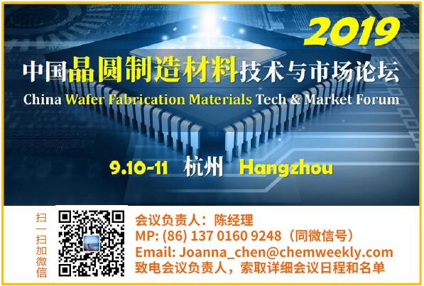
The first China wafer manufacturing material technology and market forum 2019 will be held in Hangzhou from September 10 to 11. The conference will focus on China's IC and wafer manufacturing industry policies, global and China's wafer capacity expansion and material demand outlook, China's Fab plant investment and wafer manufacturing material market, the latest technology of overseas enterprises, technology and market trends of photoresist, wet electronic chemicals, high-purity electronic gas, sputtering target materials, photomask plates, CMP materials, as well as the increasing localization rate Opportunities and challenges.
Seminar topics:
1. China's IC and wafer manufacturing industry policies
2. Global and Chinese wafer capacity expansion and material demand outlook
3. China Fab plant investment layout and wafer manufacturing material Market
4. Advanced materials and technology at home and abroad
5. Photoresist technology and market status and cutting-edge trend: KrF / ARF / EUV
6. Improvement of the localization of semiconductor wet electronic chemicals
7. Supply and demand of high-purity electronic gas and investment opportunities
8. High purity sputtering target and photomask technology and market
9. CMP material new technology and project investment
10. Development status of semiconductor silicon in China
11. Industrial visit and investigation
Scope
Costs & Precautions
Conference fee: 3200 yuan / person, 2900 yuan / person for team application (same company ≥ 3 persons); English service fee of 2000 yuan for foreign guests
Note: the fee on the day of the meeting includes: lunch, tea break, dinner, Chinese Conference information, venue tickets, etc., excluding accommodation. The accommodation fee is directly settled with the hotel before check-out. The English service fee includes: English conference information, simultaneous interpretation fee, etc. on the day of the meeting
Advertising expenses
For different plans, please contact the person in charge: Miss Chen 021-68726606-109 / 13701609248 (the same as wechat) or email to Joanna gun@
The measure of area: 350m2
Contact
- Truename:Manager Chen
- Mobile:13701609248
- E-mail:Joanna_chen@chemweekly.com
- QQ:410192892
- Address:Xinjinqiao Road, Pudong New Area, Shanghai
Disclaimer
The information on this site comes from the network and related members, and the website has done its duty to review it. Due to the uncontrollability of the process of organizing the exhibition, some of the exhibition information in the station may change the subject matter, Extending or cancelling the event, please exhibitors and visitors must check with each other again before exhibiting! All the exhibitions in this site are not hosted/co-organized or organized, if there are any disputes during the exhibition, please hold the main responsibility of the exhibition organization! QQ Email: 523138820@qq.com WeChat: 523138820 Mobile: 15313206870


HOT
-
- 2024 Shanghai International Seawater Desalination and Technology Equipment Exhibition
- 2025-12-11 To 12-13
- 2345 Longyang Road, Pudong New Area, Shanghai
-
- 2025 Shanghai Beauty Expo (Pudong) -2025 CBE Shanghai Beauty Expo
- 2025-05-22 To 05-22
- 2345 Longyang Road, Pudong New Area, Shanghai
-
- The 24th Guangzhou International Metal and Metallurgical Industry Exhibition in 2024
- 2025-05-11 To 05-13
- No. 380 Yuejiang Middle Road, Haizhu District, Guangzhou City
-
- The 24th Guangzhou International Pipe and Pipe Processing Equipment Exhibition in 2024
- 2025-05-11 To 05-13
- No. 380 Yuejiang Middle Road, Haizhu District, Guangzhou City
-
- The 24th (Die Casting Exhibition - Die Casting Exhibition) Guangzhou International Die Casting Exhibition in 2024
- 2025-05-11 To 05-13
- No. 380 Yuejiang Middle Road, Haizhu District, Guangzhou City
-
- The 24th Guangzhou International Casting Products and Casting Exhibition in 2024
- 2025-05-11 To 05-13
- No. 380 Yuejiang Middle Road, Haizhu District, Guangzhou City
-
- 2024 China Indoor Park Exhibition DIY Building Toy Exhibition Gift Toy Exhibition
- 2025-05-10 To 05-12
- No. 380 Yuejiang Middle Road, Haizhu District, Guangzhou City
-
- The 25th China International Petroleum and Petrochemical Technology and Equipment Exhibition (CIPPE) in 2025
- 2025-03-26 To 03-28
- 88 Yuxiang Road, Shunyi District, Beijing
-
- The 4th CHWE Global Cross border E-commerce Exhibition 2025
- 2025-03-20 To 03-22
- Intersection of Fuhua 3rd Road and Jintian Road in Futian District, Shenzhen City, Guangdong Province
-
- The 33rd Shanghai China International Fair in 2025
- 2025-03-01 To 03-04
- 2345 Longyang Road, Pudong New Area, Shanghai
-
- 2025 Shanghai China International Fair [Holding Time+Exhibition Address]
- 2025-03-01 To 03-04
- 2345 Longyang Road, Pudong New Area, Shanghai
-
- The 33rd China East China Import and Export Fair of the 2025 Shanghai China International Fair
- 2025-03-01 To 03-04
- 2345 Longyang Road, Pudong New Area, Shanghai
-
- 2025 Beijing Yasen Exhibition - Beijing Automotive Supplies Exhibition
- 2025-02-21 To 02-24
- 88 Yuxiang Road, Shunyi District, Beijing
-
- **2025 American Air Conditioning Refrigeration, Heating, Air Purification, Automatic Control, and Instrument Exhibition AHR
- 2025-02-10 To 02-12
- Located on highways 12 and 18 leading to the city center of Madison
-
- 2024 Guangzhou International Hotel Linen and Textile Exhibition
- 2024-12-19 To 12-21
- No. 380 Yuejiang Middle Road, Haizhu District, Guangzhou City


Expo News
- Congratulations on the grand opening of the 4th national salt product salt making equipment and packaging new material exhibition 2019 in Shanghai New International Expo Center!
- Warm congratulations on the opening of the 15th ICIF winter fine arts and crafts exhibition and 2019 China (Shenzhen) culture week in Shenzhen Convention and Exhibition Center, China!
- The audience pre registration system of the 4th Guangdong pump and valve exhibition is now on line
- Warm congratulations on the grand opening of 2019 Shanghai International Wine and spirits trade exhibition in Shanghai New International Expo Center!
- The 23rd Zhejiang (Hangzhou) Plastic Machinery Exhibition in 2024
- With the support of national policies, energy storage has become another hot area of lithium battery application, attracting a lot of capital investment. So, what is the current situation and Prospect...
- Lithium industry enters a new era, and the 2019 Shanghai lithium industry exhibition makes another success
- Congratulations on the grand opening of the 28th China (Shanghai) International wallpaper, curtain and Home Furnishing Exhibition in 2019 in Shanghai New International Expo Center!
- Congratulations on the grand opening of Shenzhen International Electronic Exhibition, embedded system exhibition and future automobile and technology exhibition in Shenzhen Convention and Exhibition C...
- The Unlimited Potential of the Western Market and the Rise of Chengdu "2024 Chengdu Electronic Information Exhibition"
- Consulting for the 2024-2025 Japan, Germany, USA, and Russia Electronic Components Exhibition
- From now on, this exhibition will be open for free for 5 days!
- Congratulations on the grand opening of the 19th China International Rubber Technology Exhibition and the 22nd International adhesive and sealant exhibition in Shanghai New International Expo Center!
- Guangzhou toy exhibition, science and education products may be concerned
- Explore the eight exhibition areas, this cross-border e-commerce exhibition in Yiwu is not simple!
- The 2024 Vietnam International Battery and Energy Storage Technology Exhibition will open on June 26th!
- Yang Jiechi attended the opening ceremony of the World Future Energy Summit and delivered a keynote speech
- Congratulations on the grand opening of 2019 packaging world (Shanghai) Expo in Shanghai New International Expo Center!
- The 20th China Environmental Expo 2019 and the 17th Shanghai international net Expo opened in Shanghai New International Expo Center
- The 4th China Private Domain Leaders Conference in 2024


