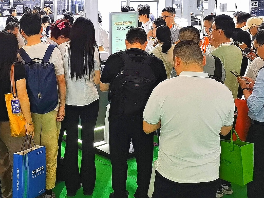





- Industry: Communications / Electronics
- Cycle: Once a year
- Time: 2027/06/16 - 06/18 (Wed To Fri Total 3 Days) Error Correction
- Address: Shanghai National Convention and Exhibition Center (Shanghai) ChinaShanghaiQingpu District No. 333 Songze Avenue, Qingpu District, Shanghai (North Gate of the Exhibition Hall)
- Sponsor:Zhongzhanbo Domain
- Organizer:Zhongzhanbo Domain


- Telephone:13162209353
- Contact:Li Yan
- Mobile:13162209353
- E-mail:2543368807@qq.com
- Address:No. 333 Songze Avenue, Qingpu District, Shanghai (North Gate of the Exhibition Hall)

INTRODUCTION
In recent years, artificial intelligence has become an important driving force for the growth of the semiconductor industry. The rapid development of computing infrastructure, from AI chips and high-performance computing to HBM, high-speed networks, and advanced packaging, is driving synchronous upgrades in multiple aspects such as chip design, wafer manufacturing, packaging testing, equipment, and materials. At the same time, the intelligence, electrification, and industrial digitization of automobiles continue to expand the demand for power semiconductors, automotive grade chips, sensors, and control chips.
From the perspective of industrial chain development, China's semiconductor industry is further strengthening its collaborative capabilities from chip design, wafer manufacturing to packaging and testing, equipment and materials. Currently, advanced packaging has become an important direction for industrial technology upgrading, and semiconductor equipment and materials continue to develop towards high-end and precision. The application space of third-generation semiconductor materials such as SiC and GaN in new energy vehicles, charging infrastructure, photovoltaic energy storage, and high-efficiency power sources is constantly expanding.
AI、 Automotive electronics and advanced packaging have become the focus of industry attention
The rapid development of the artificial intelligence industry is redefining the technological requirements of the semiconductor industry. AI training and reasoning have put forward higher requirements for computing chips, storage chips, high-speed interconnection, and advanced packaging, and have also promoted the transformation of the semiconductor industry from single chip performance competition to comprehensive capability competition of "chip+packaging+system". Industry data shows that investments in AI and high-performance computing are becoming important forces driving demand for semiconductor equipment.
Shanghai gathers industrial resources and creates a new platform for semiconductor technology exchange
As an important hub for China's integrated circuit industry, Shanghai has a solid industrial foundation and innovative resources in areas such as chip design, wafer manufacturing, packaging and testing, equipment materials, and terminal applications. Relying on the well-established electronic information and advanced manufacturing industry system in the Yangtze River Delta region, Shanghai has an important advantage in connecting upstream and downstream enterprises, research institutions, and application markets in the semiconductor industry.
Scope
Chip Design, Wafer Manufacturing, and Packaging Exhibition Area
Integrated circuit design and chip, wafer manufacturing, SiP advanced packaging, power device packaging and testing MEMS packaging and testing, silicon wafer and IC loading board, packaging substrate and application manufacturing and packaging testing EDA、MCU、 Semiconductor materials, equipment, and components for packaging and testing substrates
Exhibition Area for Semiconductor Specialized Equipment/Components
Thinning machine, single crystal furnace, grinding machine, heat treatment equipment, lithography machine, etching machine, ion implantation equipment, CVD/PVD equipment, cleaning equipment, cutting machine, mounting machine, bonding machine, testing machine, sorting machine, probe station and components, etc
Advanced Materials/Carbon Materials/Diamond Semiconductor Exhibition Area
Silicon wafers and silicon-based materials, photomasks, electronic gases, photoresist and its supporting reagents, CMP polishing materials, target materials, packaging substrates, lead frames, bonding wires, ceramic substrates, chip bonding materials, carbon based materials, diamond semiconductors, graphite materials, superhard materials, etc
Third Generation Semiconductor Exhibition Area
Nitriding (GaN) and silicon carbide (SiC), zinc oxide (ZnO) diamond, wafers, substrates and epitaxy, power devices, IGBT packaging materials, RF devices and processing equipment, etc
IC Carrier/Ceramic Substrate Exhibition Area
IC carrier board and packaging process (substrate, copper and other structural materials, dry film, gold salt and other chemicals/consumables) Chiplet packaging technology, storage, MEMS and chip applications and materials, equipment, ceramic substrate and packaging materials and equipment, etc
Component Exhibition Area
Passive components, semiconductor discrete devices/1GBT, 5G core components, special electronics, component power management, sensors, memory, connector relays, cables, plug-in devices, crystal oscillators, resistors, display devices, diodes, transistor filtering components, switches and component materials and equipment
Power Devices/Power Electronics/Automotive Semiconductors Exhibition Area
Automotive grade semiconductor control/computing chips, power semiconductors (IGBT and MOSFET), automotive grade SiC modules, power management chips, automotive electronic micro assembly and power devices, packaging and testing equipment, automation equipment, etc
Computing power, storage, artificial intelligence, CPO packaging area
Artificial intelligence chips, solutions, computing power chips and solutions, algorithm solutions, data storage, optoelectronic co packaging modules and technologies and equipment, etc
Semiconductor Display/Mini/Micro LED Exhibition Area
OLED, AMOLED, Mini/Micro LED displays, flexible displays, materials and equipment, etc
International Brand Zone
International semiconductor material suppliers, well-known equipment suppliers, well-known packaging and testing, manufacturing, contract manufacturers, etc
Costs & Precautions
Contact
- Telephone:13162209353
- Contact:Li Yan
- Mobile:13162209353
- E-mail:2543368807@qq.com
- Address:No. 333 Songze Avenue, Qingpu District, Shanghai (North Gate of the Exhibition Hall)
Disclaimer
The information on this site comes from the network and related members, and the website has done its duty to review it. Due to the uncontrollability of the process of organizing the exhibition, some of the exhibition information in the station may change the subject matter, Extending or cancelling the event, please exhibitors and visitors must check with each other again before exhibiting! All the exhibitions in this site are not hosted/co-organized or organized, if there are any disputes during the exhibition, please hold the main responsibility of the exhibition organization! QQ Email: 523138820@qq.com WeChat: 523138820 Mobile: 15313206870




 浙公安网备
浙公安网备