




- Industry: Industrial / Mechanical / Processing
- Cycle: Once a year
- Time: 2027/05/27 - 05/29 (Thur To Sat Total 3 Days) Error Correction
- Address: Hangzhou Hangzhou Grand Convention and Exhibition Center ChinaZhejiang ProvinceHangzhouXiaoshan District West of the intersection of Meishi Line and Yannan Line in Xiaoshan District, Hangzhou City
- Sponsor:Golden Exhibition Group
- Organizer:Hangzhou Sequoia Exhibition Co., Ltd


- Contact:Cai Jun
- Mobile:18621792675
- Address:West of the intersection of Meishi Line and Yannan Line in Xiaoshan District, Hangzhou City

INTRODUCTION
PCB & IME Expo 2027
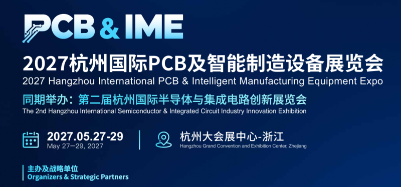
Welcome to consult | 2027 Hangzhou International PCB and Intelligent Manufacturing Equipment Exhibition
Simultaneously held: The 2nd Hangzhou International Semiconductor and Integrated Circuit Innovation Exhibition
Exhibition time: May 27-29, 2027
Exhibition Location: Hangzhou Grand Convention and Exhibition Center - Zhejiang
Exhibition Date: May 27–29, 2027Exhibition Venue: Hangzhou Grand Convention and Exhibition Center, Zhejiang
Host and partner strategic units:
Golden Exhibition Group
Zhejiang Artificial Intelligence Society
Zhejiang Semiconductor Industry Association
Zhejiang Robot Industry Development Association
Zhejiang Computer Information System Integration Industry Association
Organizers & Strategic Partners:Golden Conference & Exhibition Group
Zhejiang Artificial Intelligence Society
Zhejiang Semiconductor Industry Association
Zhejiang Robot Industry Association
Zhejiang Computer Information System Integration Industry Association
organizing unit
Hangzhou Sequoia Exhibition Co., Ltd
Hangzhou Zhiyuan Exhibition Co., Ltd
Hangzhou Changxin International Exhibition Management Co., Ltd
Co-organizers:
Hangzhou Sequoia Exhibition Co., Ltd.
Hangzhou Wisdom Source Exhibition Co., Ltd.
Hangzhou SICE International Exhibition Management Co., Ltd.
Theme: Chip board collaboration, intelligent manufacturing for the future - bridging the last mile from chips to hardware manufacturing
Theme
Chip–PCB Synergy · Shaping the Future of Intelligent Manufacturing
Bridging the Final Mile from Chips to Hardware Manufacturing
Exhibition Overview
Printed circuit boards are known as the "mother of electronic products" and are the core carrier for chips to achieve electrical interconnection. When AI computing power surges in, when new energy vehicles move forward rapidly, when third-generation semiconductors reshape industry boundaries, the demand for high-end IC carrier boards, high-frequency high-speed boards, and high multilayer boards in China continues to rise, and the process of domestic substitution accelerates. The "15th Five Year Plan" clearly proposes to accelerate the development of a new generation of intelligent manufacturing, promote the transformation of the manufacturing industry from intelligent to digital to networked, and promote the addition of new speed and achievements in "artificial intelligence+manufacturing". In the field of integrated circuits, the planning outline proposes to achieve decisive breakthroughs in key core technology research and development throughout the entire chain. The PCB industry, as a fundamental link in the electronic information manufacturing industry, is entering a policy window period of high-end, digital, and green transformation. Hangzhou and the Yangtze River Delta region provide a solid industrial hinterland for the exhibition. Hangzhou Qiantang Chip Valley has gathered over 140 integrated circuit enterprises, with an industrial scale exceeding 80 billion yuan. Its wafer manufacturing capacity accounts for more than a quarter of Zhejiang Province, making it the only county in China with the ability to manufacture wafers ranging from 4 inches to 12 inches simultaneously. The Action Plan for the Construction of "Intelligent Manufacturing Communities" in Hangzhou clearly proposes to optimize the core manufacturing links of key industries such as next-generation semiconductors and integrated circuits, embodied intelligent robots, etc. The Yangtze River Delta region gathers a large number of PCB finished product factories, material and equipment enterprises, and downstream semiconductor, computing power, and new energy industries have complete supporting facilities, possessing unique industrial location advantages.
Printed circuit boards (PCBs), often referred to as the “motherboards of electronic products,” are the core platform for electrical interconnection between chips and electronic systems. As AI computing power accelerates, new energy vehicles advance rapidly, and third-generation semiconductors reshape industry boundaries, demand for advanced IC substrates, high-frequency/high-speed PCBs, and high-layer-count boards continues to rise, accelerating the shift toward domestic alternatives.
China’s 15th Five-Year Plan calls for faster development of next-generation intelligent manufacturing, advancing the digital transformation, intelligent upgrading and networked integration of manufacturing, and driving new momentum through “AI + Manufacturing.” In the integrated circuit sector, the Plan also calls for breakthroughs in critical and core technologies across the entire value chain. As a foundational segment of electronic information manufacturing, the PCB industry is entering a strategic window for high-end, digital-intelligent and green transformation.
Hangzhou and the Yangtze River Delta provide a strong industrial base for the Expo. Hangzhou’s Qiantang Chip Valley is home to more than 140 integrated circuit companies, with the industry exceeding RMB 80 billion in scale. Its wafer manufacturing capacity accounts for more than one-quarter of Zhejiang Province’s total, making it the only county-level administrative area in China with wafer manufacturing capabilities spanning 4-inch to 12-inch wafers.
Hangzhou’s “Intelligent Manufacturing Community” Development Action Plan calls for enhanced support for core manufacturing segments across key industrial value chains, including next-generation semiconductors and integrated circuits and embodied intelligent robotics.
The Yangtze River Delta is home to a large concentration of PCB manufacturers, materials and equipment suppliers, supported by well-developed downstream ecosystems in semiconductors, AI computing and new energy. This integrated industrial landscape gives the region a distinctive location advantage and provides a strong foundation for the development of the PCB and intelligent manufacturing industries.
New Opportunities
AI computing power is rapidly pushing PCB demand towards high layers, high frequencies, and high speeds, and the industry's growth logic is shifting from scale expansion to technological improvement. At this critical juncture of industrial transformation, Gaodeng Exhibition, in collaboration with relevant industry regulatory agencies, is scheduled to hold the "2027 Hangzhou International PCB and Intelligent Manufacturing Equipment Exhibition" at the Hangzhou Grand Convention and Exhibition Center from May 27 to 29, 2027. It will be held simultaneously with the 2nd Hangzhou International Semiconductor and Integrated Circuit Industry Innovation Exhibition (Hangzhou Changxin Exhibition) at the same venue. This exhibition is positioned as a core supporting sub exhibition of Changxin Exhibition, focusing on the entire PCB industry chain and intelligent manufacturing equipment, and filling the key link of "chip substrate hardware manufacturing". Deep collaboration with the semiconductor industry chain at Changxin Exhibition: Changxin Exhibition brings together IC design, wafer manufacturing, advanced packaging Chiplet、 Third generation semiconductor and AI chip companies, a large number of chip companies urgently need to find reliable IC carrier boards and high-frequency high-speed PCB supply chains; The PCB exhibition area enables upstream chip companies to have face-to-face interactions with PCB/carrier board and intelligent manufacturing equipment companies, connecting the complete chain from chip design to hardware manufacturing. The exhibition focuses on showcasing drilling, exposure, electroplating, etching, forming, testing, and automated production lines MES、 Industrial Internet, AI quality inspection and other intelligent manufacturing equipment and programs help PCB enterprises reduce costs and increase efficiency, improve yield, and accelerate digital transformation. Aiming to fill the key link in the entire industry chain display chain of "chip design wafer manufacturing advanced packaging IC carrier board/PCB terminal hardware", build a precise docking platform between PCB and semiconductor industry, promote the localization breakthrough of high-end IC carrier board and intelligent manufacturing equipment, and inject new momentum into the high-quality development of Changsanjiao and even the national electronic circuit industry.
AI computing is rapidly driving PCB demand toward higher layer counts, higher frequencies and higher speeds, shifting the industry’s growth model from scale expansion to technology advancement.
At this critical sta of industrial transformation, Golden Conference & Exhibition Group, together with relevant industry authorities and organizations, will host the 2027 Hangzhou International PCB & Intelligent Manufacturing Equipment Expo from May 27–29, 2027, at the Hangzhou Grand Convention & Exhibition Center. The Expo will be held concurrently and in the same venue as The 2nd Hangzhou International Semiconductor & Integrated Circuit Industry Innovation Exhibition (SICE).
Positioned as a core supporting event of the SICE, the PCB Expo will focus on the entire PCB value chain and intelligent manufacturing equipment, addressing a critical link between chips, substrates and hardware manufacturing.
The Expo will work in close synergy with the Changxin Expo’s semiconductor value chain. The main expo will bring together companies across IC design, wafer manufacturing, advanced packaging, Chiplet, third-generation semiconductors and AI chips, many of which are seeking reliable supply chains for IC substrates and high-frequency/high-speed PCBs.
The PCB Expo will facilitate face-to-face business matchmaking between upstream chip companies and PCB/IC substrate manufacturers and intelligent manufacturing equipment suppliers, connecting the full chain from chip design to hardware manufacturing.
Key exhibits will include intelligent manufacturing equipment and solutions for drilling, exposure, electroplating, etching, forming, inspection and testing, automated production lines, MES, industrial internet and AI-powered quality inspection, helping PCB manufacturers reduce costs, improve efficiency and yield, and accelerate digital transformation.
The Expo aims to complete the critical link in the exhibition chain spanning chip design → wafer manufacturing → advanced packaging → IC substrates/PCBs → end-product hardware, while creating a targeted matchmaking platform connecting the PCB and semiconductor industries. It will support advances in the domestic development of high-end IC substrates and intelligent manufacturing equipment, injecting new momentum into the high-quality development of the electronic circuit industry across the Yangtze River Delta and China.
Concurrent Events
At the same time as the exhibition, multiple high-level professional events will be held, including the PCB Intelligent Manufacturing and IC Carrier Industry Summit Forum, IC Carrier Technology and Localization Replacement Seminar, PCB Intelligent Manufacturing and Digital Transformation Forum, PCB Green Manufacturing and Sustainable Development Forum, etc., bringing together industry leaders, technical experts, and industry capital to discuss cutting-edge trends. At the same time, a PCB/carrier board supply and demand matching meeting will be set up, inviting semiconductor companies, downstream terminal manufacturers, research institutes and institutions to negotiate face-to-face, promoting precise implementation of technical exchanges and business cooperation, and making exhibitions and conferences more effective.
The Expo will feature a series of high-level professional events, including the PCB Intelligent Manufacturing & IC Substrate Industry Summit, IC Substrate Technology & Domestic Development Seminar, PCB Intelligent Manufacturing & Digital Transformation Forum, and PCB Green Manufacturing & Sustainable Development Forum. Industry leaders, technology experts and investors will come together to explore emerging trends and opportunities across the sector.
A dedicated PCB/IC Substrate Supply-Demand Matchmaking Session will also be held, bringing together semiconductor companies, downstream manufacturers, research institutes and investment institutions for targeted, face-to-face discussions. The program is designed to facilitate focused technical exchange, accelerate business cooperation and deliver tangible outcomes for exhibitors and participants.
Exhibition Zones
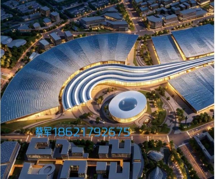
1. Circuit board finished product display area: rigid PCB, flexible FPC, rigid flex bonding board, high-frequency and high-speed board, thick copper plate, special circuit board, IC carrier board (BT/ABF), etc;
2. PCB key raw and auxiliary material area: copper-clad laminate, semi cured sheet, copper foil, ink, dry film, solder mask, electroplating chemicals, special resins, etc;
3. Intelligent manufacturing process equipment area: drilling, electroplating, pressing, etching, exposure, forming, laser processing and other equipment;
4. Detection and testing equipment area: AOI, AXI, impedance testing, flying pin testing, online detection system, etc;
5. Automated production line and digital solution area: Automated production line, AGV logistics MES、 Industrial Internet, AI quality control, environmental protection solutions, etc
6. Supply and demand docking and industrial service area: closed negotiations, industrial investment attraction, talent docking.
1. Finished PCB Products
Rigid PCBs, flexible PCBs (FPCs), rigid-flex PCBs, high-frequency/high-speed PCBs, heavy-copper PCBs, specialty PCBs, IC substrates (BT/ABF), and more.
2. Key PCB Materials & Chemicals
Copper-clad laminates (CCLs), prepregs, copper foil, inks, dry films, solder masks, plating chemicals, specialty resins, and other key materials and chemicals.
3. Intelligent Manufacturing Process Equipment
Drilling, electroplating, lamination, etching, exposure, forming, laser processing and other PCB manufacturing equipment.
4. Inspection & Testing Equipment
Automated optical inspection (AOI), automated X-ray inspection (AXI), impedance testing, flying probe testing, in-line inspection systems and other testing and inspection solutions.
5. Automated Production Lines & Digital Solutions
Automated production lines, AGV logistics systems, manufacturing execution systems (MES), industrial internet platforms, AI-powered quality control, environmental protection and waste treatment solutions, and more.
6. Business Matchmaking & Industry Services
Closed-door business meetings, investment attraction, talent matchmaking, investment and financing matchmaking, and related industry services.
Target Visitors
The organizing committee accurately invites core forces in the global electronic information industry, including IC design, advanced packaging Chiplet、 Third generation semiconductor, power devices, AI/storage chips and other semiconductor procurement and research and development personnel; PCB/FPC/IC carrier boards, copper-clad laminates, and material manufacturers' equipment procurement, process research and development, and quality departments; Manufacturers of AI servers, computing hardware, new energy vehicle electronics, communications, industrial control, and consumer electronics terminals; Automotive electronics, aerospace, and marine electronics solution providers; And software ecology, research institutes, universities, parks, institutions, industry funds, government regulatory departments, and industry organizations.
Contact Information
Cai Jun: 18621792675
Scope
Exhibition Zones
1. Circuit board finished product display area: rigid PCB, flexible FPC, rigid flex bonding board, high-frequency and high-speed board, thick copper plate, special circuit board, IC carrier board (BT/ABF), etc;
2. PCB key raw and auxiliary material area: copper-clad laminate, semi cured sheet, copper foil, ink, dry film, solder mask, electroplating chemicals, special resins, etc;
3. Intelligent manufacturing process equipment area: drilling, electroplating, pressing, etching, exposure, forming, laser processing and other equipment;
4. Detection and testing equipment area: AOI, AXI, impedance testing, flying pin testing, online detection system, etc;
5. Automated production line and digital solution area: Automated production line, AGV logistics MES、 Industrial Internet, AI quality control, environmental protection solutions, etc
6. Supply and demand docking and industrial service area: closed negotiations, industrial investment attraction, talent docking.
Costs & Precautions
Contact
- Contact:Cai Jun
- Mobile:18621792675
- Address:West of the intersection of Meishi Line and Yannan Line in Xiaoshan District, Hangzhou City
Disclaimer
The information on this site comes from the network and related members, and the website has done its duty to review it. Due to the uncontrollability of the process of organizing the exhibition, some of the exhibition information in the station may change the subject matter, Extending or cancelling the event, please exhibitors and visitors must check with each other again before exhibiting! All the exhibitions in this site are not hosted/co-organized or organized, if there are any disputes during the exhibition, please hold the main responsibility of the exhibition organization! QQ Email: 523138820@qq.com WeChat: 523138820 Mobile: 15313206870



 浙公安网备
