




- Industry: Communications / Electronics
- Cycle: Once a year
- Time: 2027/05/18 - 05/20 (Tues To Thur Total 3 Days) Error Correction
- Address: Anhui Hefei Binhu International Convention and Exhibition Center ChinaAnhui ProvinceHefei CityBaohe District 3899 Jinxiu Avenue, Baohe District, Hefei City
- Sponsor:Organizing Committee of Hefei Semiconductor and Integrated Circuit Exhibition and Beijing Zhongwei International Exhibition Co., Ltd
- Organizer:Beijing Zhongwei International Exhibition Co., Ltd., Anhui Zhongwei Exhibition Co., Ltd


- Contact:Sun Yan
- Mobile:17621568521
- E-mail:2119857701@qq.com
- Address:3899 Jinxiu Avenue, Baohe District, Hefei City

INTRODUCTION
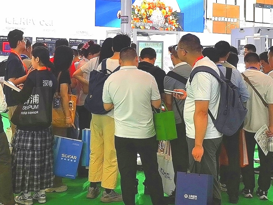
The tide of industry surges, and smart chips gather in Hefei. The 2nd Hefei Semiconductor and Integrated Circuit Industry Expo (Wanxin Exhibition) in 2027 has landed at the Binhu International Convention and Exhibition Center. The exhibition brings together industry academicians and experts, leading enterprise executives, technical chief engineers, representatives of research institutes, industry investment experts, and other industry heavyweight guests to gather industry consensus through ideological collision and explore the new future of domestic semiconductor industry development together.
The current domestic integrated circuit industry is in a critical cycle of independent innovation, with downstream markets such as AI computing power, intelligent connected vehicles, energy storage, and industrial automation continuously releasing huge demand. However, at the same time, it also faces multiple practical challenges such as material and equipment research and development, supply chain collaboration, and technology landing and mass production. How to break through technological bottlenecks, accelerate the implementation of domestic substitution, and open up channels for the transformation of industry, academia, research, and application has become a core issue of common concern in the industry, and is also the focus of discussion in the forum section of this year's Anhui Chip Exhibition.
The exhibition is accompanied by multiple high-level thematic forums, covering popular tracks such as wafer manufacturing, semiconductor key materials, advanced packaging and testing, HBM storage, third-generation semiconductors, and automotive grade chips. Industry experts from various fields took turns on stage, sharing frontline practical experience and cutting-edge research on hot topics such as mature process iteration, localization of core components, commercialization of Chiplet technology, reliability of automotive grade chips, and green semiconductor manufacturing. There is both a deep review of the current state of the industry and predictions of future trends, providing valuable industry insights for the companies present.
On site roundtable dialogue sessions were set up, where guests faced industry pain points and engaged in speculative exchanges on topics such as supply chain security, cost reduction and efficiency improvement, industry university research collaborative innovation, and breakthrough paths for small and medium-sized enterprises. On stage viewpoints clashed, while offline corporate audiences earnestly learned from their experiences. Many representatives of participating companies engaged in in-depth exchanges with guests after the forum, seeking possibilities for technical cooperation and project docking.
Unlike simply sharing technology, the Wanxin Exhibition Forum balances theoretical knowledge with practical industry experience. The guest lineup covers the upstream, midstream, and downstream of the industry chain, from upstream material and equipment manufacturers to chip design and manufacturing enterprises, and then to downstream terminal applications and capital institutions, interweaving multiple perspectives and breaking down communication barriers between technology, industry, and capital. Let cutting-edge ideas go out of the laboratory, truly connect with the actual production and operation needs of enterprises, and help enterprises find the right direction for development.
Promote development with knowledge and empower with intelligence. The intellectual feast of big names and the physical exhibits in the exhibition hall complement each other, with cutting-edge ideas on one hand and hardcore products on the other, achieving two-way empowerment of ideological exchange and business docking. Many attending companies expressed that by listening to industry experts' sharing, they have gained a clearer understanding of industry development trends and have also gained many new ideas for solving practical problems.
Based in Hefei, the IC capital of China, and linked with the industrial potential of the Yangtze River Delta. In 2027, Wanxin Exhibition will continue to build a high-end platform for exchanging ideas, gathering industry wisdom, consolidating industry synergy, and helping the domestic integrated circuit industry to achieve stability and progress, working together to enter the era of independent and controllable chips.
Scope
Scope of Exhibition: Covering the Core Field of Semiconductors
LC Design and Chip Zone
EDA full process design software, IP core, embedded system software, digital/analog/mixed signal integrated circuit design, layout design and verification services; Artificial intelligence chips (end side/edge/training), general-purpose GPU, NPU, TPU, DPU, AloT, SoC, large model training and inference chips, heterogeneous computing processors, RISC-V processor cores, high and low voltage power management chips (PMIC), industrial IoT MCU, 5G/millimeter wave RF chips, automotive grade chips (AEC-Q100 certification), secure encryption chips, storage chips (DRAM/Flash/storage control chips, high bandwidth memory HBM, storage stack chips), full category display driver chips (OLED/LCD/TCON/Mini Micro LED), integrated storage and computing chips, AI storage and computing integrated chips, intelligent vision chips; Server CPU, memory interface chip, high-speed optical module, silicon optical integration and other AI server and data center core chip products and supporting components.
Semiconductor Materials Zone
12 inch semiconductor silicon wafer (polishing/epitaxial/SOI silicon wafer), high-end photoresist (ArF/KrF/i wire) and supporting reagents, high-purity electronic chemicals, CMP polishing solution and polishing pad, high-purity metal target material (AI/Cu/Ti/Ta/W alloy target material), lithography supporting chemicals, photomask, optoelectronic chemicals, semiconductor precursor materials, special coating materials, functional thin film materials, wide bandgap compound semiconductor materials (SiC/GaN/gallium oxide substrate and epitaxial materials), high-end packaging materials (packaging substrate, lead frame, bonding wire, epoxy plastic packaging material, etc.)
◆ Packaging and Testing Measurement Zone
Covering advanced packaging technologies such as Chiplet chip heterogeneous integration, 2.5D/3D stacked packaging, TSV through silicon via process, Fan out layer out packaging, Flip chip flip chip packaging, COB packaging, vacuum eutectic, heterogeneous integration, WLCSP wafer level packaging, bumping bump manufacturing, SiP system level packaging, etc; Traditional IC packaging technology and packaging testing outsourcing services; Storage chip packaging, automotive grade high reliability packaging, power semiconductor module packaging; Integrated circuit testing equipment and technology: ATE testing system, digital/analog/mixed signal testing, high and low temperature aging testing, failure analysis equipment (SEM/EDX/FIB), wafer yield control data analysis; Sealing and testing of the entire factory and process production line, packaging equipment, testing machines, testing probe stations, and sorting machines; Electronic and communication supporting equipment, electrical instruments and meters, environmental testing equipment, analytical instruments and meters; Certification testing, automated instrumentation, and supporting solutions.
Application Ecological Zone of "Chip Screen Auto Fusion"
Display field: Mini/Micro LED, OLED, LCD new display driver technology, car display, flexible display, ultra clear high refresh rate display, integrated core chips and supporting materials under the screen; Automotive field: car specification level core chip, battery management system (BMS), car motor controller, on-board power module, on-board Ethernet chip, on-board sensor, vehicle semiconductor application solutions: industrial/AI/data center field: industrial control chip, edge computing intelligent module, AI computing module, server computing acceleration scheme, large model hardware kit, server and storage dedicated chip, industrial/car specification level sensor interface chip, memory computing integrated hardware, computing fluid temperature control system, high-speed interconnection hardware; Terminal applications: consumer electronics, robotics, security, aerospace, energy storage terminal application solutions;
Industrial support: industrial policy promotion, industrial funds, industrial park carriers, industry university research innovation achievements, product testing and certification, intellectual property and comprehensive industry support services.
Integrated Circuit Manufacturing Zone
12 inch wafer manufacturing and outsourcing, DRAM storage wafer manufacturing, display driver (DDI) wafer manufacturing, 28/40nm logic/MCU specialty processes, power device/BD/MEMS dedicated processes, IDM vertical integration whole plant project, overall construction plan for circular wafer factory, process upgrade and mass production supporting solution, MPW multi project wafer wafer fabrication service, silicon optical foundry, wafer regeneration, circular wafer testing and verification, process reliability evaluation, and mass production yield optimization services; Covering advanced GAA processes, backside power supply processes, glass packaging boards, photonic SOI and other cutting-edge new process technologies and supporting services; Mask detection, mask repair equipment, and supporting technical solutions.
Semiconductor Equipment and Core Components Zone
Front equipment: single crystal furnace, silicon crystal growth equipment, photolithography equipment, etching equipment, thin film deposition equipment (PVD/CVD/ALD), ion implantation equipment, semiconductor grade cleaning equipment, coating and developing equipment, precision measurement and testing equipment, annealing/oxidation/diffusion heat treatment equipment, photomask manufacturing equipment; Rear equipment: round thinning machine, round cutting machine, fixing machine, bonding equipment, plastic sealing equipment, cutting and forming equipment, testing and sorting machine, automatic probe station, ATE integrated circuit testing system; Core precision components: dry vacuum pump, RF power supply, electrostatic chuck (ESC), wafer transfer equipment (EFM), high-purity control valve, precision motion platform, optical components, semiconductor specific robots and automation supporting components, semiconductor precision ceramic components, cavity components, heaters, wafer bearing parts, equipment precision consumables, non-standard customized components; Complete solutions for wafer handling automation and wafer inspection automation; Ultra pure water system, clean room equipment, and supporting engineering facilities in semiconductor factories; Special gas pipeline components, vacuum valves.
◆ Third Generation Semiconductor Zone
Second and third generation compound semiconductor materials and devices: silicon carbide (SiC), gallium nitride (GaN), gallium oxide, diamond semiconductors, gallium arsenide (GaAs), indium phosphide (InP) substrates and epitaxial materials; Various power devices, RF microwave devices, high-speed communication devices, and wide bandgap semiconductor power modules; Optical chips, laser chips, optical detectors, silicon optical integrated devices, optical modules; Focusing on power semiconductor and RF communication integrated application solutions in the fields of new energy vehicles, photovoltaic energy storage, industrial power supply, high-end fast charging, 5G/6G communication, aerospace information, microwave radar, etc
Components Zone
Vehicle grade/industrial grade resistors, capacitors, potentiometers, power semiconductor discrete devices, high-end specialized connectors, heat sinks, electromechanical components; Electroacoustic devices, laser devices, electronic display devices, optoelectronic devices, industrial/automotive grade sensors, MEMS inertial, acoustic, pressure, optical sensor devices, dedicated power supplies, switches, micro motors, electronic transformers, relays; High end printed circuit boards (HDI/high-frequency/automotive grade PCBs), various specialized circuits, piezoelectric, crystal, quartz, ceramic magnetic materials; Printed circuit substrates, specialized materials for electronic functional processes, electronic adhesive (tape) products, electronic chemical materials and components; High end specialized supporting components and materials such as microwave components, communication equipment microwave materials, microwave RF detection instruments, industry-specific software, and electronic tubes.
Costs & Precautions
Contact
- Contact:Sun Yan
- Mobile:17621568521
- E-mail:2119857701@qq.com
- Address:3899 Jinxiu Avenue, Baohe District, Hefei City
Disclaimer
The information on this site comes from the network and related members, and the website has done its duty to review it. Due to the uncontrollability of the process of organizing the exhibition, some of the exhibition information in the station may change the subject matter, Extending or cancelling the event, please exhibitors and visitors must check with each other again before exhibiting! All the exhibitions in this site are not hosted/co-organized or organized, if there are any disputes during the exhibition, please hold the main responsibility of the exhibition organization! QQ Email: 523138820@qq.com WeChat: 523138820 Mobile: 15313206870



 浙公安网备
浙公安网备