




- Industry: Other Industry
- Time: 2027/05/27 - 05/29 (Thur To Sat Total 3 Days) Error Correction
- Address: Hangzhou Hangzhou Grand Convention and Exhibition Center ChinaZhejiang ProvinceHangzhouXiaoshan District West of the intersection of Meishi Line and Yannan Line in Xiaoshan District, Hangzhou City
- Sponsor:Golden Exhibition Group
- Organizer:Hangzhou Changxin International Exhibition Management Co., Ltd


- Telephone:15921089962
- Contact:Teacher Yao
- Mobile:15921089962
- Address:West of the intersection of Meishi Line and Yannan Line in Xiaoshan District, Hangzhou City

INTRODUCTION
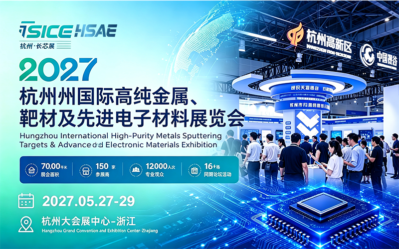
2027 Hangzhou International High Purity Metals, Target Materials and Advanced Electronic Materials Exhibition
Date: May 27-29, 2027
Location: Hangzhou Grand Convention and Exhibition Center
Host and Strategic Unit
Zhejiang Artificial Intelligence Society
Zhejiang Semiconductor Industry Association
Zhejiang Robot Industry Development Association
Zhejiang Computer Information System Integration Industry Association
Golden Exhibition Group
organizing unit
Hangzhou Changxin International Exhibition Management Co., Ltd
Simultaneously held: The 2nd Hangzhou International Semiconductor and Integrated Circuit Innovation Exhibition
Exhibition Overview
High purity metals and sputtering targets are the "invisible cornerstone" of integrated circuits, advanced packaging, AI computing chips, new displays, and power semiconductor manufacturing. Chip metalized thin films, HBM high bandwidth memory, advanced processes of 3nm and below, and Micro LED panels all heavily rely on core materials such as ultra-high purity copper, tantalum, tungsten, cobalt, and platinum group metal targets. Industry data display; The market size of sputtering target materials in China is expected to reach approximately 3.365 billion yuan by 2025, and is projected to increase to 3.8 billion yuan by 2026; It is expected that by 2027, the global market space for semiconductor sputtering targets will reach 25.1 billion yuan, and the market for display panel sputtering targets will reach 39.9 billion yuan. With the continuous expansion of domestic wafer fabs, the explosive demand for AI computing power, and the large-scale popularization of advanced packaging technology, the high-end target material market has entered a period of rising volume and price, and there is a vast space for domestic substitution of advanced process target materials. As a leading city in the national digital economy, Hangzhou has gathered a large number of chip design, AI terminal, optoelectronic display, and sensor enterprises; Zhejiang, Shanghai, and Jiangsu together form the largest integrated circuit industry corridor in China, gathering hundreds of leading enterprises in 12 inch and 8-inch wafer manufacturing, packaging and testing, panel manufacturing, and photovoltaics, forming a huge demand pool for target materials and high-purity metals procurement. Hangzhou has clearly stated that by 2027, the nine core manufacturing links of the new generation semiconductor and integrated circuit industries will basically achieve full coverage within the city.
New opportunities
To connect the entire industry chain of "materials chips" and help China's integrated circuit industry build a safe, independent, and controllable supply chain system. The organizer of the exhibition, Gaodeng Exhibition, innovatively held the 2027 Hangzhou International High Purity Metals, Target Materials, and Advanced Electronic Materials Exhibition at the same time and place as the 2nd Hangzhou International Semiconductor and Integrated Circuit Innovation Exhibition. Based on the advantages of Zhejiang's digital economy and the Yangtze River Delta integrated circuit industry cluster, the two exhibitions will be linked, focusing on the core needs of the semiconductor, display, and computing industries, connecting the entire industry chain of "high-purity metals sputtering target materials advanced electronic materials chip design manufacturing packaging and testing", creating a specialized and international top-level business and technology exchange platform for the subdivision track of high-purity target materials in China, and helping to accelerate the implementation of independent controllability and domestic substitution of key electronic materials.
Simultaneously held
To deeply empower industrial technological innovation and ecological co construction, the exhibition will host 16 high-level industry forums and special industry activities during the same period, including the Hangzhou New Era Semiconductor Development Summit Forum, Advanced Packaging and Testing Technology Forum, Semiconductor Key Materials and Equipment Innovation Forum, AI Optoelectronic Fusion and Computing Interconnection Forum, RISC-V Ecological Co construction Summit, Integrated Circuit Talent Ecological Conference, Industrial Investment Project Matchmaking Conference and a series of themed activities. The event brings together industry academicians, authoritative experts, top enterprise leaders, and senior industry investors in Hangzhou to conduct in-depth discussions on key issues such as breakthroughs in core technology bottlenecks, domestic substitution paths, and supply chain security guarantees.
target audience
The organizing committee will invite and accurately reach professionals from various fields such as semiconductors, integrated circuits, electronic power, electronic manufacturing, display manufacturing, as well as automotive, aerospace, medical and health, information and communication, and consumer electronics through diversified channels. The key invited objects cover the core links of the entire industry chain, including semiconductor wafer manufacturing, advanced packaging and testing, optical modules and AI servers, computing hardware and copper-clad PCB, new energy storage and photovoltaics, vehicle electronics, precision industrial control and high-end equipment, research institutes and material traders, terminal manufacturing general contracting enterprises, etc. Efficient docking is needed to jointly promote the collaborative innovation and high-quality development of the semiconductor and electronic materials industry.
Exhibition scope
Ultra high purity metal raw materials: 4N~7N high-purity copper, aluminum, titanium, tantalum, tungsten, molybdenum, cobalt, nickel, platinum, niobium, rare earth high-purity metals, high-purity alloys, metal powders, sputtering precursor materials, etc;
Semiconductor and display sputtering targets: flat targets, rotating tubular targets, large-size wafer specific targets, precious metal targets, barrier layer targets, interconnect targets, OLEDMicro LED specific targets, power semiconductor ceramic targets, binding backplate and welding matching, etc;
Advanced electronic supporting materials: coating consumables, vapor deposition materials, electronic pastes, ceramic substrates, packaging metal consumables, heat dissipation metal composite materials, vacuum coating auxiliary materials, etc;
Preparation and testing equipment: metal ultra-high purity purification equipment, rolling heat treatment processing equipment, vacuum binding equipment, grain detection, purity analysis, thin film performance testing instruments, residual target recovery and regeneration technology and equipment;
Semiconductors and Integrated Circuits: Integrated Circuit Design IP、EDA、 The entire industry chain includes manufacturing, packaging testing, equipment manufacturing, semiconductor materials, and more.
Exhibition participation fee
Kind reminder: For specific marketing opportunities, sponsorship plans, and booth fee standards, please contact the sales manager of the organizing unit to obtain them
A. Standard booth size of 9 square meters per unit (3M * 3M)
B. Indoor open space:
Note: Minimum rental area is 36 square meters. "Bare space" only provides exhibition area and does not include display racks, equipment, carpets, power supplies, etc.
Contact Information
Phone: 021-6047 2525
Contact: Teacher Yao
Mobile/WeChat: 159 2108 9962 (WeChat note company name+metal target exhibition)
Scope
Exhibition scope
Ultra high purity metal raw materials: 4N~7N high-purity copper, aluminum, titanium, tantalum, tungsten, molybdenum, cobalt, nickel, platinum, niobium, rare earth high-purity metals, high-purity alloys, metal powders, sputtering precursor materials, etc;
Semiconductor and display sputtering targets: flat targets, rotating tubular targets, large-size wafer specific targets, precious metal targets, barrier layer targets, interconnect targets, OLEDMicro LED specific targets, power semiconductor ceramic targets, binding backplate and welding matching, etc;
Advanced electronic supporting materials: coating consumables, vapor deposition materials, electronic pastes, ceramic substrates, packaging metal consumables, heat dissipation metal composite materials, vacuum coating auxiliary materials, etc;
Preparation and testing equipment: metal ultra-high purity purification equipment, rolling heat treatment processing equipment, vacuum binding equipment, grain detection, purity analysis, thin film performance testing instruments, residual target recovery and regeneration technology and equipment;
Semiconductors and Integrated Circuits: Integrated Circuit Design IP、EDA、 The entire industry chain includes manufacturing, packaging testing, equipment manufacturing, semiconductor materials, and more.
Costs & Precautions

Contact
- Telephone:15921089962
- Contact:Teacher Yao
- Mobile:15921089962
- Address:West of the intersection of Meishi Line and Yannan Line in Xiaoshan District, Hangzhou City
Disclaimer
The information on this site comes from the network and related members, and the website has done its duty to review it. Due to the uncontrollability of the process of organizing the exhibition, some of the exhibition information in the station may change the subject matter, Extending or cancelling the event, please exhibitors and visitors must check with each other again before exhibiting! All the exhibitions in this site are not hosted/co-organized or organized, if there are any disputes during the exhibition, please hold the main responsibility of the exhibition organization! QQ Email: 523138820@qq.com WeChat: 523138820 Mobile: 15313206870





 浙公安网备