



- Industry: Communications / Electronics
- Cycle: Once a year
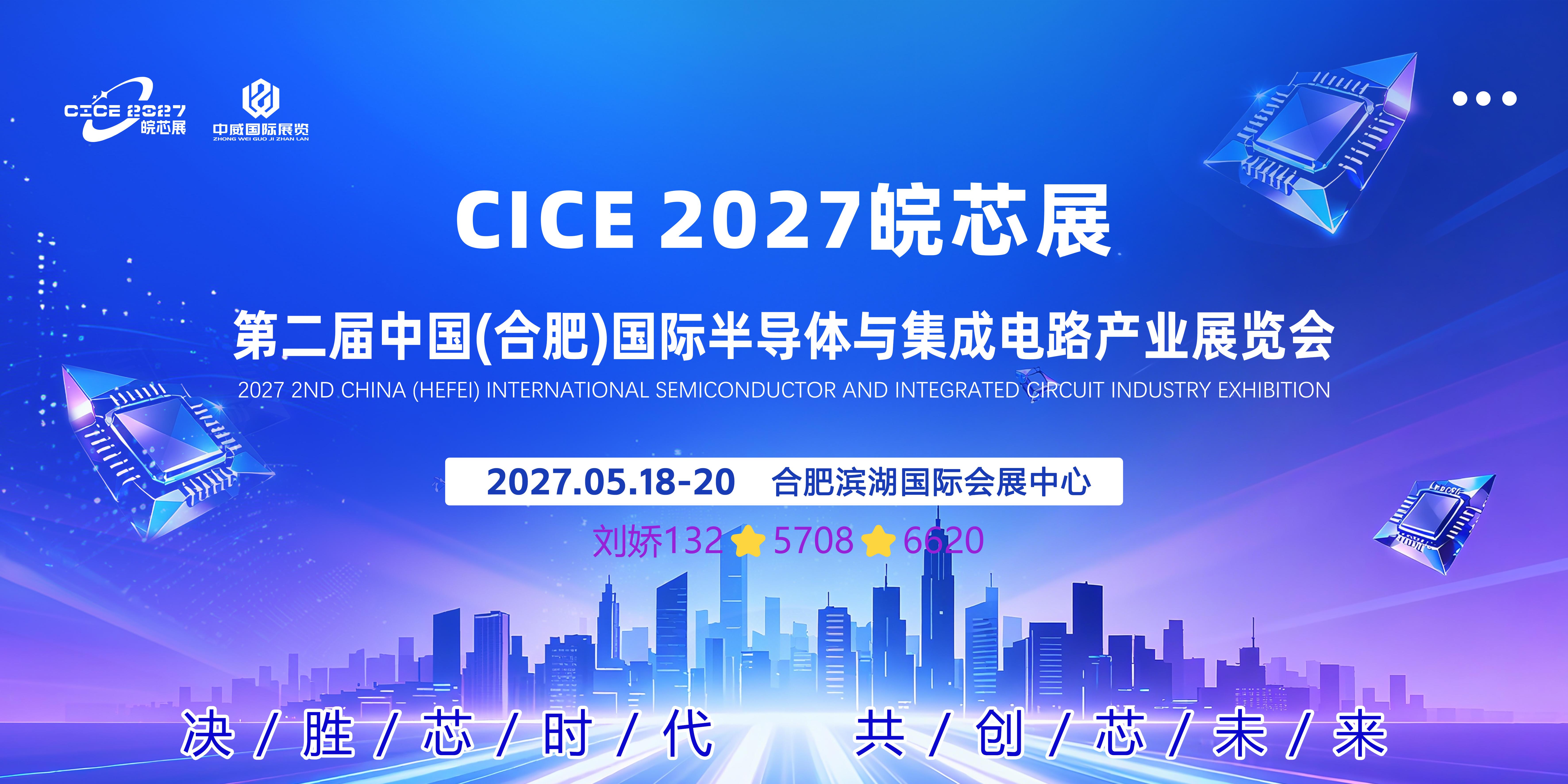
- Time: 2027/05/18 - 05/20 (Tues To Thur Total 3 Days) Error Correction
- Address: Anhui Hefei Binhu International Convention and Exhibition Center ChinaAnhui ProvinceHefei CityBaohe District 3899 Jinxiu Avenue, Baohe District, Hefei City
- Sponsor:Beijing Zhongwei International Exhibition Co., Ltd
- Organizer:Zhongwei Exhibition


- Contact:Liu Jiao
- Mobile:13257086620
- Address:3899 Jinxiu Avenue, Baohe District, Hefei City

INTRODUCTION
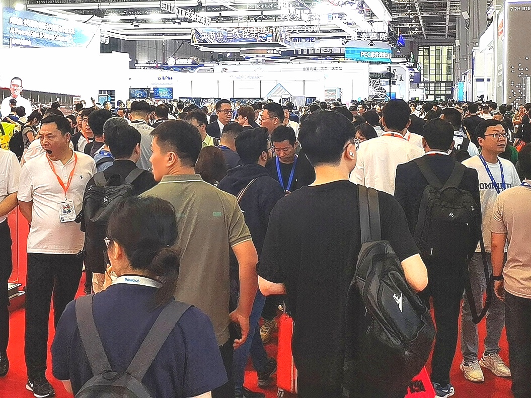
Against the backdrop of the deep adjustment of the global semiconductor industry pattern and the continuous acceleration of domestic integrated circuit localization, regional industrial clustering, industrial chain synergy, and localized technological innovation have become the core trends of industry development. Hefei, as a national key integrated circuit industry base, relies on the hard core industry matrix of "chip screen integration and lifelong intelligence" to gather thousands of upstream and downstream supporting semiconductor enterprises, forming a complete industrial closed loop from materials, equipment, design, manufacturing to packaging and testing, and terminal applications. It is the core carrier of the semiconductor industry in the central region with the largest scale, most complete supporting facilities, and strongest innovation vitality.
To further activate the industrial potential in the central region, break down the collaborative barriers between upstream and downstream of the industrial chain, and connect cutting-edge technologies with market applications,2027 Hefei Semiconductor Industry ExhibitionHeavy landing. The exhibition is based on the industrial foundation of Hefei, radiating to the entire market of Central and East China, focusing on the innovation and upgrading of the semiconductor industry and precise supply-demand docking. It creates a professional and large-scale industry platform that integrates technology display, new product release, business negotiation, industry investment promotion, and academic exchange, helping the domestic semiconductor industry break through technological bottlenecks, fill in supporting shortcomings, and expand application markets.
This exhibition closely follows the current hot track and development pain points of the semiconductor industry, covering core areas such as power semiconductors, advanced packaging, automotive grade chips, AI chips, semiconductor materials and equipment with precision. It gathers leading domestic and foreign enterprises, specialized and innovative enterprises, universities and research institutes, terminal procurement enterprises, and industry authoritative institutions. With professional exhibitions as carriers, it comprehensively showcases the latest technological achievements, mass-produced products, and overall solutions of the semiconductor industry, and builds an efficient, accurate, and high-quality resource docking bridge for industry practitioners.
1、 Core highlights of the exhibition
This exhibition relies on the unique industrial advantages of Hefei and is different from traditional industry exhibitions. It focuses on three core features: "industry rooting, scene landing, and precise empowerment". On the one hand, it deeply caters to the needs of terminal industries such as new energy vehicles, new displays, intelligent equipment, and photovoltaic energy storage in Hefei, achieving precise matching between chip technology and local application scenarios, and enabling technological innovation to take effect; On the other hand, we will focus on the core track of domestic substitution, highlighting the industrialization achievements of domestic materials, equipment, and chips, and helping small and medium-sized science and technology innovation enterprises connect with the market and resources.
At the same time, the exhibition is accompanied by multiple high-level industry summits, technical seminars, supply and demand matching sessions, and investment promotion activities. Industry experts, business leaders, and investment experts are invited to interpret industry policies, analyze industry trends, and share cutting-edge technologies, providing comprehensive empowerment for participating enterprises in technology iteration, market expansion, investment and financing cooperation, industry university research transformation, and promoting the improvement and upgrading of the central semiconductor industry cluster.
2、 Full dimensional exhibition scope (covering the entire industry chain)
The exhibition strictly follows the ecological layout of the entire semiconductor industry chain, covering upstream core materials and equipment, midstream chip design, wafer manufacturing, advanced packaging and testing, downstream multi field terminal applications, and full chain industry supporting services. It comprehensively displays the full ecological achievements of the integrated circuit industry. The specific exhibition scope is as follows:
1. Chip Design and IC Product Exhibition Area
Covering various types of general and specialized integrated circuit products, including automotive grade, industrial grade, and consumer grade chips, specifically including artificial intelligence computing chips, image processing chips, storage chips, RF communication chips, analog signal chips, digital control chips, power management chips, power chips, sensor chips, security encryption chips, etc. Simultaneously covering the entire chip design chain supporting services, including EDA design tools, semiconductor IP authorization, layout design, chip simulation verification, testing and calibration, customized chip research and development solutions, etc.
2. Exhibition Area for Wafer Manufacturing and Featured Processes
Focusing on the field of semiconductor wafer production and process iteration, showcasing various wafer products such as 6/8/12 inch general-purpose wafers, special function wafers, epitaxial wafers, etc; Covering core process technologies and optimization solutions such as photolithography, etching, thin film deposition, ion implantation, polishing, and cleaning. Simultaneously showcasing production supporting technologies and services such as specialty process outsourcing, advanced process research and development, wafer yield improvement, process reliability testing, mass production yield optimization, and chip failure analysis, covering mature processes, specialty processes, and cutting-edge advanced processes.
3. Semiconductor Core Materials Exhibition Area
Comprehensive coverage of key materials for semiconductor production and manufacturing, including traditional silicon-based materials such as monocrystalline silicon wafers, polished silicon wafers, epitaxial wafers, SOI silicon wafers, etc; Third generation wide bandgap semiconductor materials: silicon carbide, gallium nitride, gallium oxide, aluminum nitride, sapphire substrate, etc. At the same time, various key auxiliary materials such as photoresist, mask, high-purity electronic special gas, metal target, wet electronic chemicals, grinding and polishing materials, packaging substrates, packaging resins, conductive pastes, insulation materials, etc. will be exhibited, focusing on the domestic substitution results of domestic semiconductor materials.
4. Exhibition Area for Semiconductor Specialized Equipment and Accessories
Showcasing specialized equipment for semiconductor production, processing, and testing throughout the entire process, including front-end wafer manufacturing equipment, mid-range process processing equipment, and back-end packaging and testing equipment, mainly including lithography machines, etching machines, thin film deposition equipment, ion implantation machines, precision cleaning equipment, detection and measurement equipment, sorting equipment, bonding equipment, cutting equipment, MOCVD equipment, etc. At the same time, supporting products and services such as core equipment components, precision consumables, automation control systems, intelligent detection instruments, equipment maintenance, equipment renovation and upgrading, and overall production line solutions will be exhibited.
5. Advanced Packaging and Testing Technology Exhibition Area
Focusing on current mainstream advanced packaging technologies and traditional packaging and testing processes, we will showcase cutting-edge packaging technologies and products such as Chiplet chip packaging, SiP system level packaging, 2.5D/3D stacked packaging, TSV through-hole packaging, FlipChip flip chip packaging, Fan out fan out packaging, etc. Simultaneously covering traditional lead packaging, power device packaging, MEMS sensor packaging, optoelectronic chip packaging and other processes, supporting the display of packaging and testing equipment, testing probes, automated testing systems, reliability testing, high and low temperature aging testing, electromagnetic compatibility testing, failure analysis and other full chain packaging and testing services.
6. Terminal Application and Industrial Supporting Exhibition Area
Focusing on the multi scenario application of semiconductors, showcasing the terminal products and system solutions of integrated circuit products in fields such as new energy vehicles, intelligent networking, autonomous driving, photovoltaic wind energy storage, industrial automation, intelligent robots, artificial intelligence computing centers, new displays, 5G/6G communication, smart homes, medical electronics, aerospace, and the Internet of Things. At the same time, it gathers supporting service resources such as investment promotion, financing institutions, qualification testing and certification, intellectual property services, transformation of scientific research achievements in universities, talent cultivation, and industry consulting in industrial parks, to build a complete semiconductor industry service ecosystem.
3、 The Value and Future Prospects of the Exhibition Industry
The 2027 Hefei Semiconductor Industry Exhibition is based on the origin of the industry, focusing on the real economy, with the core purpose of "linking industrial resources, empowering technological innovation, and accelerating domestic substitution". Relying on the perfect industrial ecology and huge terminal application market in Hefei, it connects the key channels of supply and demand matching, technology transformation, and industrial investment attraction in the industrial chain. The exhibition will continue to gather high-quality semiconductor enterprises and innovative resources from across the country, promote collaborative cooperation, technological complementarity, and resource sharing between upstream and downstream enterprises, and help solve industry pain points such as supply-demand mismatch, high technological barriers, and high docking costs.
In the future, the exhibition will continue to deeply cultivate the semiconductor industry track in central China, gathering merchants through exhibitions, promoting research through conferences, and revitalizing the city through industry. It will continue to help Hefei build a highly influential innovation and industrial agglomeration highland for the integrated circuit industry in the country, injecting a continuous stream of new momentum for the independent, controllable, high-quality, and sustainable development of China's semiconductor industry in central China.
Scope


Costs & Precautions
Contact
- Contact:Liu Jiao
- Mobile:13257086620
- Address:3899 Jinxiu Avenue, Baohe District, Hefei City
Disclaimer
The information on this site comes from the network and related members, and the website has done its duty to review it. Due to the uncontrollability of the process of organizing the exhibition, some of the exhibition information in the station may change the subject matter, Extending or cancelling the event, please exhibitors and visitors must check with each other again before exhibiting! All the exhibitions in this site are not hosted/co-organized or organized, if there are any disputes during the exhibition, please hold the main responsibility of the exhibition organization! QQ Email: 523138820@qq.com WeChat: 523138820 Mobile: 15313206870


 浙公安网备
浙公安网备