




- Industry: Communications / Electronics
- Cycle: Once a year
- Time: 2027/05/27 - 05/29 (Thur To Sat Total 3 Days) Error Correction
- Address: Hangzhou Hangzhou Grand Convention and Exhibition Center ChinaZhejiang ProvinceHangzhouXiaoshan District West of the intersection of Meishi Line and Yannan Line in Xiaoshan District, Hangzhou City
- Sponsor:Zhejiang Semiconductor Industry Association
- Organizer:Hangzhou Changxin International Exhibition Management Co., Ltd


- Contact:organizing committee
- Mobile:13917789060
- Address:West of the intersection of Meishi Line and Yannan Line in Xiaoshan District, Hangzhou City

INTRODUCTION
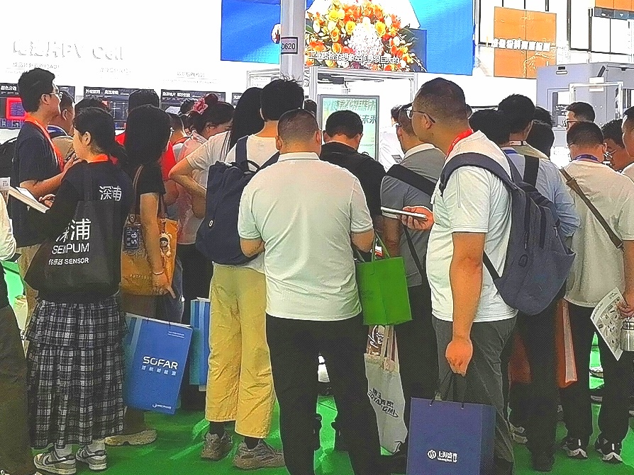
2027 Hangzhou International Photolithography and Electronic Chemicals Exhibition
Simultaneously held: The 2nd Hangzhou International Semiconductor and Integrated Circuit Innovation Exhibition
Exhibition time: May 27-29, 2027
Exhibition Location: Hangzhou Grand Convention and Exhibition Center - Zhejiang
Approved by: Ministry of Commerce of the People's Republic of China
Host: Zhejiang Semiconductor Industry Association
Shanghai Gaodeng Exhibition Group Co., Ltd
Organizer: Hangzhou Changxin International Exhibition Management Co., Ltd
Exhibition Overview
As China's integrated circuit industry enters a critical stage of high-quality development and localization substitution. Core key materials such as photoresist, ultra-high purity wet electronic chemicals, and electronic specialty gases are the core weaknesses that constrain breakthroughs in advanced domestic processes and ensure the security of the semiconductor industry supply chain. They are also key areas that China's integrated circuit industry urgently needs to overcome. Among them, photoresist is known as the "pearl on the crown of semiconductor materials", and electronic chemicals are the core "industrial blood" of chip manufacturing. Their technological breakthroughs and industrialization are directly related to the independent, controllable, and safe development of China's chip industry. In order to thoroughly implement the national integrated circuit industry development strategy, accelerate the localization process of key semiconductor materials, improve the industrial supporting system, and promote the construction of strong, supplementary, and extended industrial chains, the 2027 Hangzhou International Photolithography and Electronic Chemicals Exhibition and the 2nd Hangzhou International Semiconductor and Integrated Circuit Innovation Exhibition will be held simultaneously at the Hangzhou Grand Convention and Exhibition Center under the coordination of the organizing committee. The exhibition is themed "Material Innovation · Future of Chip Chain", based on the advantages of the world-class integrated circuit industry cluster in the Yangtze River Delta region. It innovatively adopts the dual exhibition linkage mode of "Key Materials Special Exhibition+Semiconductor Full Industry Chain Exhibition", focusing on the technological iteration, production line certification, and supply and demand docking of photoresist, wet electronic chemicals, and special electronic materials. It connects the entire industry chain of upstream materials, core equipment, wafer manufacturing, advanced packaging and testing, and terminal applications, accurately builds a specialized platform integrating technical exchange, commercial docking, achievement transformation, and project cooperation, empowers the independent and controllable semiconductor material supply chain, helps the industry cultivate new quality productivity, and promotes the high-quality innovation and development of China's integrated circuit industry.
Exhibition Highlights
1) Industry benchmark exhibition, filling the gap in segmented fields
This exhibition is the first specialized and international brand exhibition in China that focuses on the sub sectors of photoresist and electronic chemicals. It accurately anchors the core demand for domestic production of semiconductor key materials, fills the gap in vertical exhibitions in the industry, and creates an annual industry technology benchmark and core platform for commercial and trade docking.
2) Dual exhibition linkage empowerment, building a closed-loop of the entire industry chain
Double exhibitions will be held simultaneously in the same venue and resources will be interconnected, achieving deep linkage between the semiconductor key materials special exhibition and the full industry chain innovation exhibition. Covering the entire process of material research and development, equipment matching, wafer manufacturing, and packaging and testing applications, helping participating companies face wafer fabs directly IDM、 Core procurement, process, and R&D teams of packaging and testing enterprises and IC design enterprises achieve precise and efficient docking.
3) High end forums gather strength to deepen the integration of industry, academia, research and application
At the same time as the exhibition, more than 10 high-end thematic forums were held, including the China Photolithography and Electronic Chemicals Industry Conference and the Yangtze River Delta Semiconductor Key Materials Innovation and Development Conference. Academicians, experts, industry leaders, and executives of leading enterprises gathered to conduct in-depth discussions on core issues such as technological breakthroughs, production line verification, standard specifications, and supply-demand coordination, empowering industry technological innovation and the implementation and transformation of achievements.
4) Supported by the core location, it gathers the advantages of industrial clusters
The exhibition will be held in Hangzhou, the core city of the semiconductor industry in the Yangtze River Delta region. It will connect with major industrial centers such as Shanghai, Suzhou, Wuxi, and Hefei, and rely on multi-level industrial support policies at the provincial and municipal levels to gather regional industries, talents, and capital resources. It will provide enterprises with a one-stop empowerment platform for industrial agglomeration, policy docking, market expansion, and project investment.
5) Global resource convergence, creating an international cooperation window
The exhibition gathers top photoresist and electronic chemical companies and research institutions from around the world, inviting international professional buyers and technical teams to participate and exchange ideas, building a high-quality platform for international technology exchange, business cooperation, and brand expansion, and helping domestic industries connect with the global market.
target audience
This exhibition is aimed at inviting professional visitors in the field of integrated circuits and semiconductor materials nationwide, with a focus on inviting investment personnel from various economic and information departments and semiconductor industry parks; Various industrial funds and investment and financing institutions; Wafer fab IDM、 Storage factory, advanced packaging and testing, panel and PCB head enterprise process, procurement and R&D personnel; Employees in IC design, semiconductor equipment, and core component enterprises; Photoresist and resin PAG、 Upstream raw material enterprises such as monomers, and semiconductor specialty chemical enterprises such as wet electronic chemicals and electronic specialty gases; A supporting enterprise specializing in chemical purification, filtration, storage, transportation, and testing equipment, as well as technology research and development and achievement transformation personnel from major universities and research institutes, will participate in the exhibition and conference.
Contact Information
Phone: 13917789060
Scope
Exhibition Scope
1. The entire photoresist industry chain: semiconductor photoresist, display/PCB photoresist, upstream raw materials for photoresist, photolithography supporting reagents, and photolithography related supporting materials;
2. Wet electronic chemicals: ultra-high purity sulfuric acid, hydrogen peroxide, ammonia water, hydrofluoric acid, developing solution, etching solution, stripping solution, cleaning solution; Electronic grade solvents, MO sources, precursors, chelating agents, etc; Chemical purification, distillation, filtration technology, etc;
3. Electronic specialty chemicals: electronic specialty gases, polishing fluid CMP, target material supporting chemicals, packaging chemical materials, conductive adhesives, special photolithography supporting polymer materials, etc;
4. Production, purification, testing and equipment: electronic chemical synthesis, distillation, purification, filtration and transportation, closed storage and transportation; Ultra high purity testing, particle size analysis, and impurity detection instruments; Clean systems, hazardous chemical safety handling equipment, etc;
5. Transformation of Industry University Research Achievements: Achievements from photolithography materials and electronic chemical laboratories in universities and research institutes, technology transfer, joint research and development project exhibitions, etc;
6. Semiconductors and Integrated Circuits: Covering IC Design EDA、 The complete industrial chain includes wafer manufacturing, advanced packaging and testing, semiconductor equipment, third-generation semiconductors, AI chips, computing hardware, automotive grade semiconductors, semiconductor core components, and industrial park investment and financing services.
Costs & Precautions
Contact
- Contact:organizing committee
- Mobile:13917789060
- Address:West of the intersection of Meishi Line and Yannan Line in Xiaoshan District, Hangzhou City
Disclaimer
The information on this site comes from the network and related members, and the website has done its duty to review it. Due to the uncontrollability of the process of organizing the exhibition, some of the exhibition information in the station may change the subject matter, Extending or cancelling the event, please exhibitors and visitors must check with each other again before exhibiting! All the exhibitions in this site are not hosted/co-organized or organized, if there are any disputes during the exhibition, please hold the main responsibility of the exhibition organization! QQ Email: 523138820@qq.com WeChat: 523138820 Mobile: 15313206870


 浙公安网备
浙公安网备