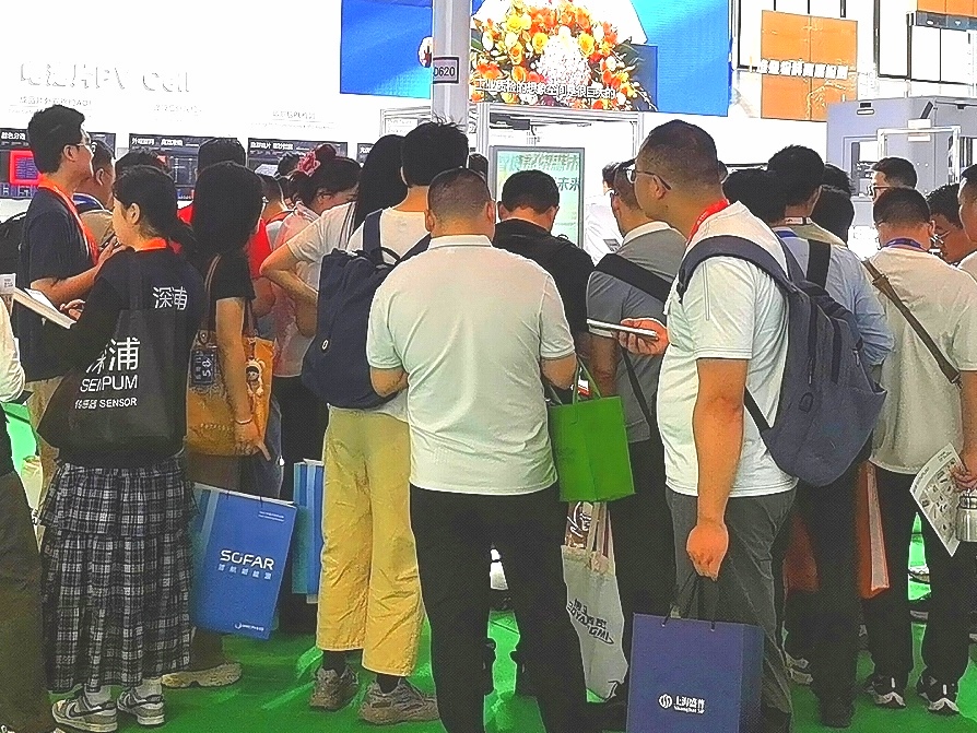





- Industry: Communications / Electronics
- Cycle: Once a year
- Time: 2027/05/18 - 05/20 (Tues To Thur Total 3 Days) Error Correction
- Address: Anhui Hefei Binhu International Convention and Exhibition Center ChinaAnhui ProvinceHefei CityBaohe District 3899 Jinxiu Avenue, Baohe District, Hefei City
- Sponsor:Organizing Committee of Hefei Semiconductor and Integrated Circuit Exhibition and Beijing Zhongwei International Exhibition Co., Ltd
- Organizer:Beijing Zhongwei International Exhibition Co., Ltd., Anhui Zhongwei Exhibition Co., Ltd


- Company:Beijing Zhongwei International Exhibition Co., Ltd
- Contact:Sun Yan
- Mobile:17621568521
- E-mail:2119857701@qq.com
- Address:3899 Jinxiu Avenue, Baohe District, Hefei City

INTRODUCTION
The global semiconductor industry is undergoing a deep reshuffle, with domestic integrated circuits gradually shifting from passive catch-up to independent innovation, while undertaking the current wave of localization substitution in the trillion dollar market and laying out cutting-edge technology tracks for the future. Rooted in the fertile land of the "chip screen automotive integration" industry in Hefei, the 2027 Wanxin Exhibition is based on the advantages of the Yangtze River Delta industrial hub. With professional exhibitions as industrial links, it connects the existing development achievements, current market opportunities, and long-term technological blueprints of the domestic semiconductor industry, and builds a comprehensive platform for the entire industry chain to showcase achievements, supply and demand docking, technical discussions, and resource cooperation. It witnesses the complete and advanced path of the local chip industry from small to large and from weak to strong.
Looking back at the present, it is a crucial stage for the landing and application of domestic semiconductors, as well as the acceleration of large-scale substitution. The four trillion level downstream markets of artificial intelligence, new energy storage, intelligent connected vehicles, and industrial automation continue to release massive procurement demands, becoming the most core shipping battlefield for domestic chips at the current stage. The computing power chips, third-generation semiconductor power devices, automotive grade controllers, and industrial control simulation chips that were once monopolized by overseas products for a long time are now rapidly being replaced in major terminal devices. However, there are still pain points in the domestic industrial chain: the disconnect between upstream and downstream information makes it difficult for chip design companies to quickly connect with high-quality end customers; Small and medium-sized wafer fabs and packaging manufacturers lack stable orders, and cutting-edge technology solutions lack landing scenarios; The technical communication channels between upstream and downstream enterprises are limited, which restricts the efficiency of product iteration.
In 2027, Wanxin Exhibition will face the existing problems in the industry and break down barriers in the upstream and downstream of the entire industry chain. The exhibition covers upstream core links such as EDA design software, semiconductor raw materials, wafer manufacturing equipment, various self-developed chips, packaging and testing. At the same time, it gathers a large number of downstream purchasers such as AI computing power manufacturers, energy storage machine enterprises, automotive companies, and automation equipment manufacturers, creating a one-stop face-to-face negotiation scene. Exhibitors can visually display their current mass-produced products, quickly obtain commercial orders, and enable mature domestic chips to firmly grasp the current market dividends, transforming technological achievements into actual production capacity and revenue, and consolidating the basic foundation of the domestic semiconductor industry. Multiple specialized supply-demand matchmaking sessions will be held at the exhibition site to accurately match supply and demand resources, shorten product sample, certification, and mass production cycles, and accelerate the current process of domestic substitution.
Based on the exhibition and looking to the future, Wanxin Exhibition also undertakes the mission of cutting-edge technology exchange and industry foresight layout. The semiconductor industry is experiencing rapid technological iteration, and next-generation technologies such as Chiplet chip integration, advanced processes, wide bandgap semiconductors, onboard advanced chips, and industrial high reliability chips will determine the competitive voice of the domestic industry in the coming years. Relying solely on existing mature products to seize the existing market is far from enough. Only by laying out cutting-edge research and development in advance can we overcome the dilemma of long-term follow-up development.
This exhibition is accompanied by multiple heavyweight industry summit forums, inviting industry experts, research institutions, and technical leaders of leading enterprises to share their themes and conduct in-depth discussions on cutting-edge technology routes, industry development trends, and technical challenges. The exhibition specifically sets up a cutting-edge innovation exhibition area, open to display seats for start-up chip companies and research institutes, showcasing the new generation of products that are still in the research and development testing stage. Relying on the industry talents and capital resources gathered at the grand event, high-quality innovative projects can connect with industrial capital, solve the problem of R&D funding, enable cutting-edge technologies to step out of the laboratory, steadily promote the industrialization process, and build a solid technological foundation for the long-term development of domestic semiconductors.
As a regional benchmark semiconductor professional exhibition, the 2027 Wanxin Exhibition is not just a simple product exhibition and sales event, but also a bridge connecting the present and future industries. At present, it leverages existing industrial chain resources, helps mature chip products seize the four trillion dollar market, and steadily promotes domestic substitution; Looking towards the future, it gathers cutting-edge innovation forces, exchanges advanced technology directions, incubates new generation semiconductor products, and continues to fill the gaps in the domestic industrial chain.
Relying on the mature industrial clusters in Hefei and the vast application market in the Yangtze River Delta, Wanxin Exhibition in 2027 will continue to leverage its platform value, connect the upstream and downstream of the industrial chain, industrial capital, and research institutions, accompany the domestic semiconductor industry to deeply cultivate the market, focus on breaking through technological bottlenecks in the future, and jointly embark on a new journey of high-quality development of the integrated circuit industry.
Scope
Ic Design and Chip Zone
EDA full process design software, IP core, embedded system software, digital/analog/mixed signal integrated circuit design, layout design and verification services; Artificial intelligence chips (end/edge/training), general-purpose GPUs, NPUs, TPUs, DPUs, AI SoCs, large model training and inference chips, heterogeneous computing processors, high and low voltage power management chips (PMIC), industrial IoT MCUs, 5G/millimeter wave RF chips, automotive grade chips (AEC.Q100 certified), secure encryption chips, storage chips (DRAM/Flash/storage control chips, high bandwidth memory HBM, storage stack chips), full category display driver chips (OLED/LCD/TCON/Mini MicroLED), integrated storage and computing chips, AI storage and computing fusion chips, intelligent vision chips; Server CPU, memory interface chip, high-speed optical module, silicon optical integration and other AI server and data center core chips and supporting components.
Semiconductor Materials Zone
12 inch semiconductor silicon wafer (polishing/epitaxial/SOI silicon wafer), high-end photoresist (ArF/KrF/wire) and supporting reagents, high-purity electronic special gas, CMP polishing solution and polishing pad, high-purity metal target material (AI/Cu/Ti/Ta/W alloy target material), photolithography supporting chemicals, photomask, wet electronic chemicals, semiconductor precursor materials, special coating materials, functional thin film materials, wide bandgap compound semiconductor materials (SiC/GaN/gallium oxide substrate and epitaxial materials), high-end packaging materials (packaging substrate, lead frame, bonding wire, epoxy encapsulation material, etc.)
Advanced Packaging and Testing Zone
Chiplet chip heterogeneous integration technology, 2.5D/3D stacked packaging, TSV through silicon via process, Fan out fan out packaging, WLCSP wafer level packaging, Bumping bump manufacturing, SiP system level packaging; Specialized packaging and testing for storage chips, automotive grade high reliability packaging, and power semiconductor module packaging; Integrated circuit testing equipment and technology: ATE fully automated testing system, digital/analog/mixed signal testing, high and low temperature aging testing system, failure analysis equipment (SEM/EDX/FIB), wafer yield control and data analysis system.
Application Ecological Zone of "Chip Screen Auto Fusion"
Display field: Mini/Micro LEDO.LED.LCD new display driver technology, car displays, flexible displays, ultra clear high refresh rate displays, integrated core chips and supporting materials under the screen; In the automotive field: automotive grade core chips, battery management systems (BMS), automotive motor controllers, and onboard power modules; Industry/AI/data center: industrial control chip, edge computing intelligent module, AI computing module, server computing acceleration scheme, large model hardware supporting, server and storage dedicated chips, industrial/vehicle gauge level sensor interface chip: industrial supporting: industrial policy promotion, industrial fund, industrial park carrier, innovation achievements of industry, university and research, product testing and certification, intellectual property rights and industrial comprehensive supporting services.
Integrated Circuit Manufacturing Zone
12 inch wafer manufacturing and outsourcing, DRAM storage wafer manufacturing, display driver (DI) wafer manufacturing, 28/40nm logic/MCU specialty processes, power device/BD/MEMS dedicated processes, IDM vertical integration whole plant project, overall wafer plant construction plan, process upgrade and mass production supporting solution, wafer regeneration, wafer testing and verification, process reliability evaluation, and mass production yield optimization services; Covering advanced GAA processes, backside power supply processes, glass packaging substrates, photonic SOI and other cutting-edge new process technologies and supporting services; Mask detection, mask repair equipment, and supporting technical solutions.
Semiconductor Equipment and Core Components Zone
Front equipment: lithography equipment, etching equipment, thin film deposition equipment (PVD/CVD/ALD), ion implantation equipment, semiconductor grade cleaning equipment, coating and developing equipment, precision measurement and testing equipment, annealing/oxidation/diffusion heat treatment equipment:
Rear equipment: wafer thinning machine, wafer cutting machine, solidification machine, bonding equipment, plastic packaging equipment, rib cutting and forming equipment, testing sorting machine, automatic probe station, ATE integrated circuit testing system;
Core precision components: dry vacuum pump, RF power supply, electrostatic chuck (ESC), wafer transfer equipment (EFEM), high-purity control valve, precision motion platform, optical components, semiconductor specific robots and automation supporting components, semiconductor precision ceramic components, cavity components, heater, circular bearing accessories, equipment precision consumables, non-standard customized components; Complete solutions for wafer handling automation and wafer inspection automation; Ultra pure water system, clean room equipment, and supporting engineering facilities in semiconductor factory buildings.
Third Generation Semiconductor Zone
Second and third generation compound semiconductor materials and devices: silicon carbide (SiC), gallium nitride (GaN), gallium oxide, gallium arsenide (GaAs), indium phosphide (InP) substrates and epitaxial materials, various power devices, RF microwave devices, high-speed communication devices, and wide bandgap semiconductor power modules; Focusing on the overall application solutions of power semiconductors and RF communication in the fields of new energy vehicles, photovoltaic energy storage, industrial power supply, high-end fast charging, 5G/6G communication, aerospace information, microwave radar, etc.
Components Zone
Vehicle grade/industrial grade resistors, capacitors, potentiometers, power semiconductor discrete devices, high-end specialized connectors, heat sinks, electromechanical components; Electroacoustic devices, laser devices, electronic display devices, optoelectronic devices, industrial/automotive grade sensors, dedicated power supplies, switches, micro motors, electronic transformers, relays; High end printed circuit boards (HDI/high-frequency/automotive grade PCBs), various specialized circuits, piezoelectric, crystalline, quartz, ceramic magnetic materials; Printed circuit substrates, specialized materials for electronic functional processes, electronic adhesive (tape) products, electronic chemical materials and components; High end specialized supporting components and materials such as microwave components, communication equipment microwave materials, microwave RF detection instruments, industry-specific software, and electronic tubes.
Costs & Precautions
Contact
- Company:Beijing Zhongwei International Exhibition Co., Ltd
- Contact:Sun Yan
- Mobile:17621568521
- E-mail:2119857701@qq.com
- Address:3899 Jinxiu Avenue, Baohe District, Hefei City
Disclaimer
The information on this site comes from the network and related members, and the website has done its duty to review it. Due to the uncontrollability of the process of organizing the exhibition, some of the exhibition information in the station may change the subject matter, Extending or cancelling the event, please exhibitors and visitors must check with each other again before exhibiting! All the exhibitions in this site are not hosted/co-organized or organized, if there are any disputes during the exhibition, please hold the main responsibility of the exhibition organization! QQ Email: 523138820@qq.com WeChat: 523138820 Mobile: 15313206870



 浙公安网备
浙公安网备