


- Industry: Communications / Electronics
- Time: 2026/11/12 - 11/14 (Thur To Sat Total 3 Days) Error Correction
- Address: Beijing Beijing National Convention Center ChinaBeijingChaoyang District Beijing Chaoyang District Beichen Road Olympic Park
- Sponsor:China Semiconductor Industry Association, China Electronic Information Industry Development Research Institute
- Organizer:China Semiconductor Industry Association, China Electronic Information Industry Development Research Institute


- Telephone:159 0177 7585
- Contact:Liu Wei
- Mobile:159 0177 7585
- Address:Beijing Chaoyang District Beichen Road Olympic Park

INTRODUCTION


2026 China Semiconductor Expo | Semiconductor Materials Exhibition | Semiconductor Equipment Exhibition
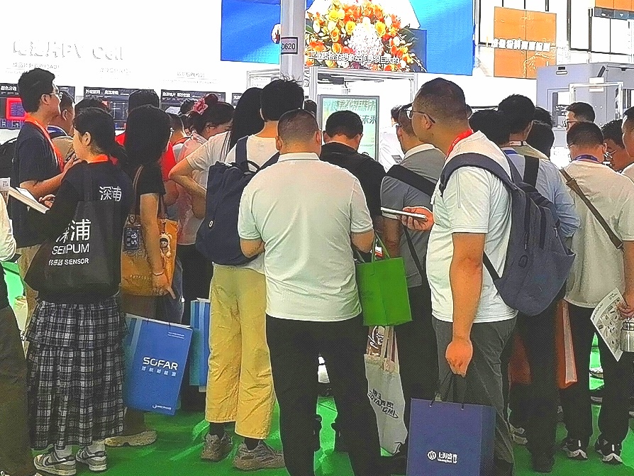
The 23rd China International Semiconductor Expo
Date: November 12-14, 2026
Location: Beijing National Convention Center
Hosted by: China Semiconductor Industry Association, China Institute of Electronic Information Industry Development
Since 2003, the China International Semiconductor Expo (IC China) has been the most significant and professional landmark event in China's semiconductor industry, and has become a top-level industry brand event and benchmark. Relying on the industry appeal, resource organization, and corporate cohesion of the China Electronics Information Industry Development Research Institute and the China Semiconductor Industry Association at home and abroad, we will build a global development bridge for precise docking of the upstream and downstream of the regional semiconductor and integrated circuit industry chain, as well as production, supply, and marketing enterprises.
The main theme of this expo is "panoramic chain display, terminal application empowerment, and leading enterprise driving". It focuses on the latest technologies, products, and applications in the upstream and downstream of the integrated circuit industry chain, with a focus on showcasing artificial intelligence chips, advanced manufacturing processes, key materials and equipment, hot application scenarios, etc. It showcases the chain, ecosystem, and scene. At the same time, highlighting the use of exhibitions to lead and promote exhibitions, closely linking exhibition activities, mobilizing the enthusiasm of enterprises, professional audiences, and ordinary visitors to participate, promoting multi-party and diversified cooperation, and enhancing the popularity of exhibitions.
The exhibition content is mainly based on the industrial chain foundation of semiconductor materials, equipment, design, manufacturing, packaging and testing, and extends to application terminals such as artificial intelligence, automobiles, and robots. As the innovative highlight of this exhibition, it focuses on leading enterprises in the application end and creates an immersive interactive zone and experience space driven by IC key application scenarios. The overall style highlights a sense of technology, futurism, and interactivity, allowing visitors to intuitively experience the disruptive changes that chips bring to production and life.
Exhibition Area Planning:
The exhibition covers an area of 50000 square meters and includes seven exhibition areas:
Display content:
Semiconductor equipment manufacturing: packaging equipment, diffusion equipment, welding equipment, cleaning equipment, testing equipment, refrigeration equipment, oxidation equipment, thinning machine, cutting machine, surface mount machine, single crystal furnace, oxidation furnace, grinding machine, heat treatment equipment, lithography machine, etching machine, polishing machine, chamfering machine, ion implantation equipment CVD/PVD equipment, coating/developing machines, front-end testing equipment, wet process equipment, thermal processing, coating equipment, single crystal deposition systems, solidification machines, plasma cleaning equipment, cutting machines, mounting machines, bonding machines, wire bonding machines, plastic packaging machines, reflow soldering, wave soldering, testing machines, bending equipment, sorting machines, robot automation, machine vision, other materials and electronic specialized equipment, coupling machines, carrier forming machines, testing equipment, constant temperature and humidity test chambers, sensors, packaging molds, testing fixtures, precision slide tables, stepper motors, valves, probe stations, clean room equipment, water treatment, etc;
Semiconductor materials: silicon wafers and silicon-based materials, silicon wafers, silicon wafers, monocrystalline silicon, silicon wafers, germanium silicon materials, S01 materials, silicon materials and compound semiconductor materials for solar cells, quartz products, graphite products, anti-static materials, photoresist and its supporting reagents, crystal tape, photomask plates, electronic gases, special chemical gases, CMP polishing materials, packaging substrates, lead frames, bonding wires, encapsulation materials, ceramic substrates, chip bonding materials, photoresist materials, wet electronic chemicals, sputtering targets, sealing materials, slicing, grinding plates, polishing plates, thin films, etc;
Third generation semiconductors: Third generation semiconductors such as silicon carbide (SiC), gallium nitride (GaN), wafers, substrates, packaging, testing, optoelectronic devices (LED), laser (LD), detector ultraviolet), power electronic devices (diode, MOSFET, JFET, BJT, IGBT, GTO, ETO, SBD, HEMT, etc.), microwave and radio frequency devices (HEMT, MMIC), etc;
IC design: IC and related electronic product design, IC product and application technology, IC testing methods and testing instruments, IC design and design tools, IC manufacturing and packaging, EDA, IP design, embedded software, digital circuit design, analog and mixed signal circuit design, integrated circuit layout design, IDM, Fabless factory, etc;
◆ Wafer Manufacturing and Packaging: Wafer Manufacturing, SiP Advanced Packaging OSATs、EMS、OEMs、IDM、 Silicon wafers and IC packaging carriers, printed circuit boards, packaging substrates and equipment, assembly and testing, packaging design, testing, equipment and application manufacturing and packaging testing, etc EDA、MCU、 Printed circuit boards, packaging substrates, semiconductor materials and equipment, etc;
Integrated circuit manufacturing: wafer manufacturing plants, wafer foundries, analog integrated circuits, digital integrated circuits, mixed signal integrated circuit manufacturing, integrated circuit terminal products, etc;
◆ Packaging and testing accessories: testing probe station, probe card, testing machine, sorting machine, packaging equipment, packaging substrate, lead frame bonding wire, lead bonding, soldering testing, automation testing, laser cutting and others, grinding fluid, cutting fluid, sealing film (adhesive) high-temperature tape, laminated substrate, patch adhesive, feeding board, solder wire flow control, quartz graphite, silicon carbide, etc;
◆ Electronic components: resistors, capacitors, potentiometers, electronic tubes, heat sinks, electromechanical components, connectors, semiconductor discrete devices/IGBTs, electroacoustic devices, laser devices, electronic display devices, optoelectronic devices, sensors, power supplies, switches, micro motors, electronic transformers, relays, printed circuit boards, integrated circuits, various circuits, piezoelectricity, crystals, quartz, ceramic magnetic materials, printed circuit substrates, electronic functional process specific materials, electronic adhesive (tape) products, electronic chemical materials and components, passive devices, 5G core components, special electronics, components, power management, storage, connectors, cables, plug-in devices, crystal oscillators, resistors, potentiometer magnetic components, filtering components PCB board, motor fan, electroacoustic device, display device, diode, transistor filter element, switch and component materials and equipment, etc;
2026 China International Semiconductor Expo Organizing Committee
Contact: Liu Wei 159 0177 7585 (same as V)
Scope


Costs & Precautions
Contact
- Telephone:159 0177 7585
- Contact:Liu Wei
- Mobile:159 0177 7585
- Address:Beijing Chaoyang District Beichen Road Olympic Park
Disclaimer
The information on this site comes from the network and related members, and the website has done its duty to review it. Due to the uncontrollability of the process of organizing the exhibition, some of the exhibition information in the station may change the subject matter, Extending or cancelling the event, please exhibitors and visitors must check with each other again before exhibiting! All the exhibitions in this site are not hosted/co-organized or organized, if there are any disputes during the exhibition, please hold the main responsibility of the exhibition organization! QQ Email: 523138820@qq.com WeChat: 523138820 Mobile: 15313206870


