


- Industry: Industrial / Mechanical / Processing
- Time: 2026/12/09 - 12/11 (Wed To Fri Total 3 Days) Error Correction
- Address: Shanghai Shanghai New International Expo Center (SNIEC) ChinaShanghaiPudong New Area No. 2345 Longyang Road, Pudong New Area, Shanghai
- Sponsor:2026 Shanghai International Nanotechnology and Application Exhibition
- Organizer:2026 Shanghai International Nanotechnology and Application Exhibition


- Telephone:136 8165 8788
- Contact:Liang Jiajin
- Mobile:136 8165 8788
- Address:No. 2345 Longyang Road, Pudong New Area, Shanghai

INTRODUCTION


2026 Shanghai International Nanotechnology and Application Exhibition
Date: December 9-11, 2026
Location: Shanghai New International Expo Center
Exhibition Review
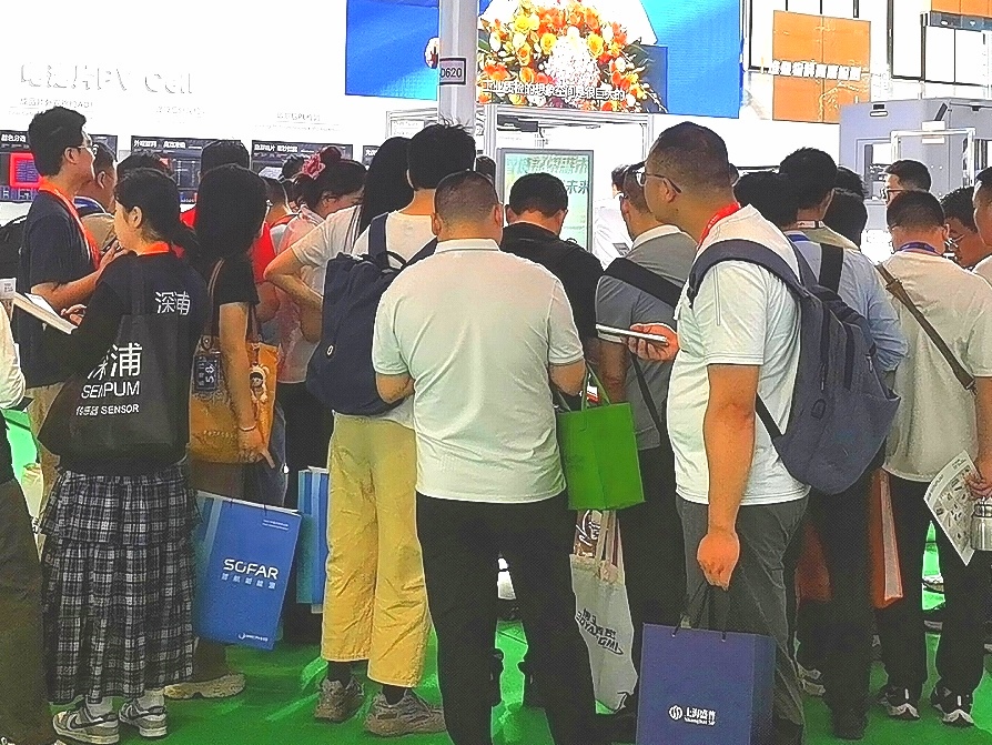
The previous exhibition covered an area of 30000 square meters and attracted over 400 companies from around the world. A total of 28862 people from more than 20 countries and regions visited. Nanjing Julong, Baoding Technology, Baotailong, China Bao'an, Tiannai Technology, Guoci Materials, Wanshun New Materials, Pulite, Defang Nano, Keliyuan, Tongji Technology, ST Ruide, CR Micro, Ziguang Guowei, Sida Semiconductor, Siwei Tuxin, Yangjie Technology, Quanzhi Technology, New Clean Energy, OFILM, Xingan Intelligence, Yingbo Scientific Instruments, Hongyang Technology, Baiteng Technology, Oxford Instruments, Shengke Nano, Nandun, Saint Gobain, Antonpa, Beaver, Nanotechnology, Xianfeng Nano, Xirui Electronics, Hanwei Technology, Yijing Technology NanoPow AS、 Minxin Microelectronics Nanomakers、 Wuxi Weigan Silex、Admatechs、 Famous enterprises such as Dazu Laser, Xinlun New Materials, Chujiang New Materials, and Feiwotai have been invited to participate in the exhibition.
industry event
The 2026 Shanghai International Nanotechnology and Application Exhibition focuses on the upstream and downstream industries of nanotechnology, including micro nano manufacturing, third-generation semiconductors, nano new materials, flexible printed electronics, nano imprinting, inkjet printing, and nano health. It aims to create an excellent stage for enterprise display, product promotion, capital cooperation, technology docking, and exchange. During this period, we will invite leading figures from the global business community, top nanotechnology experts and institutions from various research institutes, and representatives from government agencies to exchange and share the latest achievements, cutting-edge information, and development trends in popular fields upstream and downstream of the nanotechnology industry.
The 2026 Shanghai International Nanotechnology and Application Exhibition will be grandly held from December 9th to 11th, 2026 at the Shanghai New International Expo Center! It will attract over 400 companies from more than 20 countries and regions including Germany, the United States, the United Kingdom, France, the Netherlands, China, Japan, and South Korea to participate in the exhibition. Through exhibition resources, we invite decision-makers from national, provincial, municipal, and relevant research institutions, electronics, semiconductors, optoelectronic devices, advanced manufacturing, thin films, coatings, energy storage batteries, supercapacitors, plastics and rubber, composite materials, electromagnetic shielding, sensors, biomedicine, environmental engineering, information, electronics, new energy, new materials, microelectronics, machinery, textiles, coatings, inks, automotive parts, marine engineering, corrosion prevention, national defense, aerospace, aviation, chemical and other industries to discuss and exchange international application technologies on the use and research and development of "nanotechnology", enhance the overall competitiveness of the industry, promote and improve the application and manufacturing level of nanotechnology in China.
As a globally influential event in the field of nanotechnology, this conference will adhere to the exhibition purpose of "highlighting brands, exploring innovation, focusing on practical results, and strengthening services". With unique creativity, scientific and reasonable integration and dissemination, and excellent services, it will provide a "high-level, high-grade, and high-quality" exhibition and communication stage for exhibitors with a new concept, and create a large-scale event in the industry. We look forward to your participation in this exhibition!
Exhibition Highlights
※ Focus on the key links of intelligent manufacturing to depict the digital production revolution: in order to comply with the digital production and manufacturing era, the exhibition will provide more industrial Internet, industrial cloud platform, nanotechnology and other solutions to meet the market needs.
※ Deeply reaching application fields to unleash efficient productivity of enterprises: The exhibition will comprehensively cover various fields of intelligent manufacturing practice, providing one-stop digital solutions for advanced manufacturing, new energy vehicles, aerospace, consumer electronics, biomedicine, electronic appliances, semiconductors, energy storage batteries, environmental protection, textiles and other industries.
The intelligent manufacturing vitality platform drives Industry 4.0: The exhibition scale has exceeded 30000 square meters, and the exhibitor lineup is upgrading, bringing various advanced nano products and cutting-edge technologies to jointly build a more powerful industrial manufacturing and trade platform.
※ Rich seminar activities collide with new inspirations in the nanotechnology industry: The three-day seminar agenda will be led by industry experts to survey the trends in the nanotechnology market and stimulate new thinking in intelligent manufacturing.
Reason for participation
Drive benchmark convergence: As an international professional event in the nanotechnology industry, nanotechnology is the most important showcase. Like a magnet, it attracts and gathers internationally renowned enterprises, innovative small and medium-sized enterprises, and start-up enterprises to jointly focus on the key topics in the industry and explain the enormous importance of nanotechnology for future production applications. Committed to building a docking platform for global exhibitors and buyers to upgrade their 'smart' manufacturing.
Dynamic market changes: The exhibition attracted over 400 industry leaders from multiple countries and regions, including Germany, the United States, the United Kingdom, France, the Netherlands, China, Japan, and South Korea, with an exhibition area of 30000 square meters. The three-day exhibition is expected to attract a total of 28862 professional visitors, greatly promoting international exchanges in the nanotechnology market and the development of the trade market. The exhibition not only provides opportunities for numerous international brands to enter the Chinese and Asian markets, but also brings a global procurement platform to the Chinese market.
Future trend display: Shanghai International Nanotechnology Exhibition has promoted the development of China's nanotechnology industry. Every year, the exhibition focuses on real-time hot topics in the industry, showcasing cutting-edge products, technologies, and innovative solutions, gathering industry professionals and experts, monitoring future development trends, and leading the industry towards continuous breakthroughs and upgrades in intelligent manufacturing.
A hundred media outlets have been tracking and reporting on the entire process
This exhibition places great emphasis on shaping and promoting the brand of exhibitors. By inviting central media, mainstream financial media, large portal websites, industry media, and overseas media to provide comprehensive, multi-dimensional, and three-dimensional coverage of exhibitors, it promotes new products and technologies to global buyers and creates unlimited business opportunities for exhibitors. This exhibition will invite hundreds of media including CCTV, Xinhua News Agency, China Business News, China Securities News, Securities Times, Shanghai Securities News, Phoenix, Sohu, NetEase, Sina, Tencent, Tiktok, etc.
Exhibition Scope
《1》 New nano materials/carbon nano materials: (graphene, fullerene, carbon nanotubes), nano metals and their oxide materials (nano gold, nano silver, nano aluminum oxide, nano iron oxide, etc.), nano powder materials, carbon nanotubes, nano fibers, nano microspheres, nano coatings, nano ceramics, electrodes, nano composites, nano biomaterials, nano optical materials, gallium nitride substrate materials, nano grinding equipment (dry wet grinding, horizontal sand grinder, bead sand grinder, three rod grinder), nano particle mixtures, dispersion technology materials, etc.
《2》 Micro nano manufacturing and sensors: nano grinding equipment (dry wet grinding, horizontal sand mill, bead sand mill, three bar grinder), nano particle mixtures, dispersion technology, thin film manufacturing technology, MEMS technology and applications, etching, ion beam laser processors, electron beam processing, ion beam processing, nano transistor technology, filling and charging processing, microcircuit manufacturing, ultra precision surface processing technology, fusion bonding technology, next-generation lithography technology, flexible and printed electronics technology, inkjet manufacturing and 3D printing technology, embossing technology, femtosecond laser exposure equipment, emulsification, bonding, inkjet printers, sensors, nanoelectronics, optoelectronics, jets, models, WCM, etc;
Analysis and testing: optical microscope, SPM, AFM, LSI test detector, ultra precision measuring instrument, design tool, simulation, electron microscope (SEM/TEM), analysis equipment, molecular imaging, 3D measurement, X-ray CT, molecular design software, pressure platform, probe, electric furnace, white light interferometer, ellipsometer, ZETA potential analysis, laboratory powder preparation and testing instruments (laser particle size analyzer, particle counter, etc.);
《3》 Third generation semiconductors and applications, gallium nitride (GaN) and silicon carbide (SiC), zinc oxide (ZnO), diamond and other third-generation semiconductor substrates, epitaxial materials, photoresist, photomask, CMP polishing materials, photoresist materials, wet electronic chemicals and other semiconductor materials, semiconductor production, packaging and other electronic specialized equipment, compound semiconductor RF devices, power devices, LED lighting displays and other upstream and downstream industrial chains and innovative applications;
《4》 Flexible printed electronics, synthesis, preparation, and characterization of organic and inorganic electronic inks, processing and printing of thin film organic-inorganic transistors, thin film solar cells, printing and preparation of organic and inorganic light-emitting devices, printed displays (OLED, quantum dots, electronic paper), printed sensors, textile electronics, printing flexible, stretchable, wearable electronic technology, printing and preparation of PCB and RFID antennas, packaging of organic, flexible, and printed electronic devices, nanomaterial printing technology, etc;
Pricing
Exhibiting projects: Domestic enterprises, joint ventures, foreign-funded enterprises
Standard booth (3m * 3m) 15800 yuan/piece 17800 yuan/piece 4000 US dollars/piece
Double opening booth (3m * 3m) 17800 yuan/piece 19800 yuan/piece 4500 US dollars/piece
Light land (minimum rent of 36 m2) 1700 yuan/m2 1900 yuan/m2 400 US dollars/m2
Standard booth: (3M x 3M) booth (including three side panels, fascia board, one table and two chairs, 220V power sockets, carpet, cleaning fees, etc.).
Open space: does not include any supporting facilities, and can be rented separately if needed.
Exhibition Tips
1. Please fill out the "Exhibition Application and Contract" form carefully and fax it to the organizing committee with the official seal.
2. After applying for a booth, exhibitors are required to wire transfer the booth fee to the designated account of the conference within 3 working days. After the remittance, please fax the remittance receipt to the organizing committee for verification; If payment is not made in a timely manner within the specified time, the organizing committee will not reserve the original booth.
3. The principle of booth sequence allocation is "apply first, pay first, arrange first".
4. In order to ensure the overall image of the conference, the organizing committee reserves the final right to adjust the booths of some exhibitors.
contact information
Shanghai Xuntong Exhibition Co., Ltd
Phone:+86-21-5415 5272
Contact: Liang Jiajin 136 8165 8788 (same WeChat account)
Scope


Costs & Precautions
Contact
- Telephone:136 8165 8788
- Contact:Liang Jiajin
- Mobile:136 8165 8788
- Address:No. 2345 Longyang Road, Pudong New Area, Shanghai
Disclaimer
The information on this site comes from the network and related members, and the website has done its duty to review it. Due to the uncontrollability of the process of organizing the exhibition, some of the exhibition information in the station may change the subject matter, Extending or cancelling the event, please exhibitors and visitors must check with each other again before exhibiting! All the exhibitions in this site are not hosted/co-organized or organized, if there are any disputes during the exhibition, please hold the main responsibility of the exhibition organization! QQ Email: 523138820@qq.com WeChat: 523138820 Mobile: 15313206870


