


- Industry: Communications / Electronics
- Cycle: Once a year
- Time: 2026/05/22 - 05/24 (Fri To Sun Total 3 Days) Error Correction
- Address: Anhui Hefei Binhu International Convention and Exhibition Center ChinaAnhui ProvinceHefei CityBaohe District 3899 Jinxiu Avenue, Baohe District, Hefei City
- Sponsor:Beijing Zhongwei
- Organizer:Beijing Zhongwei International Exhibition Co., Ltd


- Contact:Liu Jiao
- Mobile:13257086620
- Address:3899 Jinxiu Avenue, Baohe District, Hefei City

INTRODUCTION


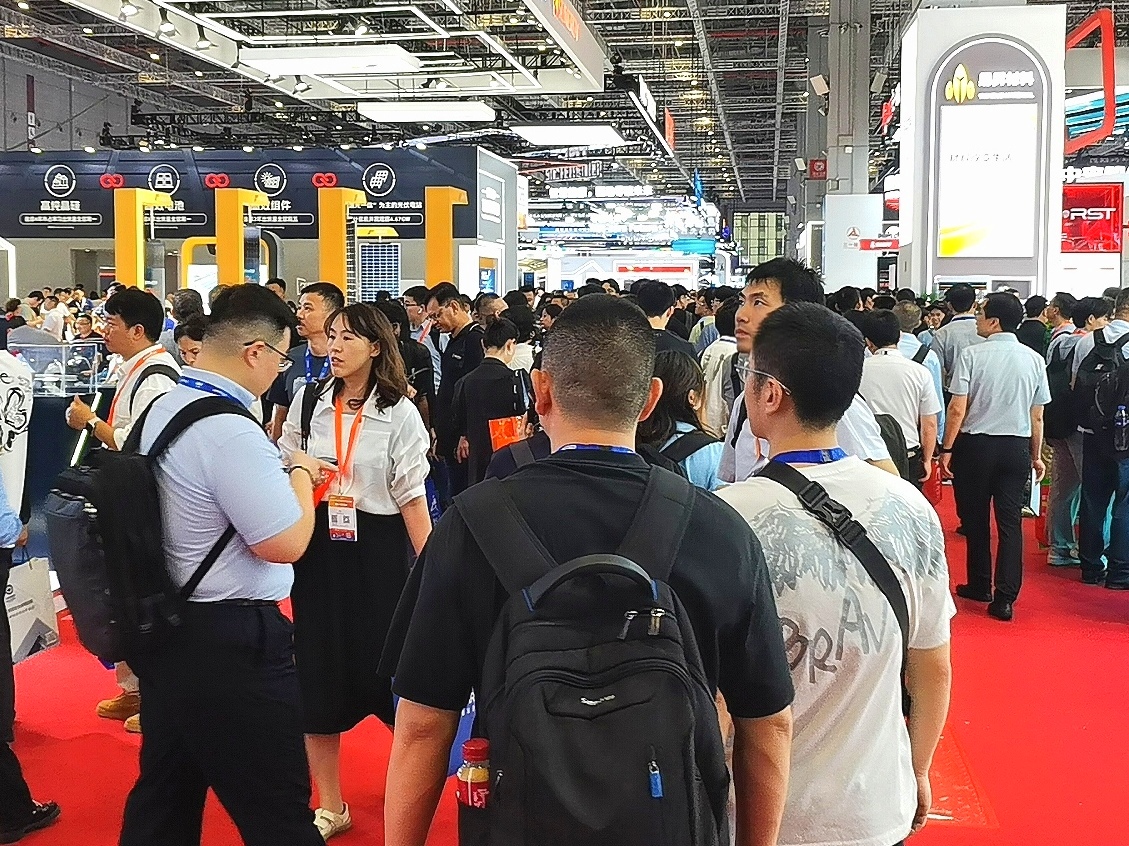
The 2026 China (Anhui) International Semiconductor and Integrated Circuit Industry Exhibition will grandly open from May 22-24, 2026 at the Binhu International Convention and Exhibition Center in Hefei. At the exhibition site, there is a dazzling array of cutting-edge technologies and innovative products. From the ingenious conception of chip design to the meticulous craftsmanship of manufacturing processes; From the pursuit of excellence in packaging testing to the innovation of equipment materials, we present the development achievements and latest trends of the semiconductor industry in all aspects. Not only that, a variety of forums, seminars, and technical exchange meetings are being held simultaneously. Guests from all walks of life, including industry, academia, and research, express their opinions and jointly explore the challenges and opportunities faced by the industry's development, accurately assess the pulse of industry development, and consolidate consensus for moving forward.
Exhibition Scope
1. Ic Design/Chip Zone
EDA, IP design, embedded software, digital circuit design, analog and mixed signal circuit design, integrated circuit layout design, IDM, Fabless factory, artificial intelligence chips, power management chips, IoT chips, 5G communication chips and solutions, automotive electronic chips, security control chips, mixed signal communication RF chips, storage chips, LED lighting and display driver chips, etc;
2. Wafer Manufacturing and Packaging Zone:
Wafer manufacturing, SiP advanced packaging OSATs、 EMS、OEMs、IDM、 Silicon wafers and IC packaging carriers, printed circuit boards, packaging substrates and equipment, assembly and testing, packaging design, testing, equipment and application manufacturing and testing, and packaging testing EDA、MCU、 Printed circuit boards, packaging substrates, semiconductor materials and equipment, etc;
3. Integrated Circuit Manufacturing Zone
Manufacturing of wafer fabs, wafer foundries, analog integrated circuits, digital integrated circuits, and mixed signal integrated circuits;
4. Third Generation Semiconductor Zone
Third generation semiconductor materials such as silicon carbide (SiC), gallium nitride (GaN), wafers, substrates, packaging, testing, optoelectronic devices (LED, laser LD, detector UV), power electronic devices (diode, MOSFET, JFET, BJT, IGBT, GTO, ETO, SBD, HEMT, etc.), microwave RF devices (HEMT, MMIC), etc.
5. Semiconductor Materials Zone
Silicon wafers, silicon chips, photoresists, wafer tapes, photomasks, electronic gases, CMP polishing materials, photoresist materials, wet electronic chemicals, sputtering targets, packaging materials, slicing, grinding, polishing, thin films, silicon wafers and silicon-based materials, photomask templates, high-purity gases, electronic specialty gases, wet electronic chemicals, photoresists and their supporting reagents, CMP polishing materials, target materials, packaging substrates, lead frames, bonding wires, encapsulation materials, ceramic substrates, chip bonding materials, fluids, valves, etc; 6. Equipment Manufacturing Zone
Thinning machine, single crystal furnace, oxidation furnace, grinding machine, heat treatment equipment, lithography machine, etching machine, ion implantation equipment, CVD/PVD, PECVD equipment, coating and developing machine, detection equipment, cleaning equipment, cutting machine, mounting machine, bonding machine, testing machine, sorting machine, probe station, clean room equipment, water treatment, etc;
7. Packaging Testing Zone
Packaging and testing equipment, packaging and testing process line enterprises, testing probe stations, testing machines, sorting machines, packaging equipment, packaging substrates, lead frame bonding wires, etc;
8. Electronic Components Zone
Resistors, capacitors, potentiometers, electronic tubes, heat sinks, electromechanical components, connectors, semiconductor discrete devices, electroacoustic devices, laser devices, electronic display devices, optoelectronic devices, sensors, power supplies, switches, micro motors, electronic transformers, relays, printed circuit boards, integrated circuits, various circuits, piezoelectricity, crystals, quartz, ceramic magnetic materials, printed circuit substrates for printed circuits, electronic functional process specific materials, electronic adhesive (tape) components, electronic chemical materials and parts, etc;
9. AI+5G Zone
Industrial Internet platform, intelligent robot, smart factory, smart car networking, smart phone, intelligent transportation, aerospace electronics, smart home appliances, UAV, 5G development and application, multi access edge computing, network slicing, virtual technology, medical electronics, etc;
10. Smart Power Zone
Microwave RF, semiconductor LED, ion power supply, shared smart charging, communication power supply, photovoltaic/wind power/energy storage power supply design, power converter magnetic technology, etc;
11. Comprehensive exhibition area
Government groups from all over the country, high-tech industrial parks related to semiconductors, securities, banks, insurance, funds, investment and financial institutions, etc.
professional visitor
1. Senior leaders and technical leaders of integrated circuit design, manufacturing, packaging and testing, semiconductor materials, equipment and other upstream and downstream enterprises in the semiconductor industry, as well as technology and equipment research and development and production enterprises, distributors, agents, service providers, traders, etc;
2. 5G applications, big data, Internet of Things, intelligent connected vehicles, intelligent driving, automotive electronics, vehicle and automotive parts factories, lithium batteries, next-generation computing, consumer electronics, new energy, artificial intelligence computing infrastructure, intelligent equipment and robots, etc;
3. Senior leaders and technical leaders of terminal application enterprises such as aerospace, defense and military industry, radar, medical, photovoltaic, optical communication, and optical modules;
Park: Demonstration Zone, Industrial Park, Science and Technology Park, Entrepreneurship Park, etc.
Industry chain enterprises: financial companies, investment companies, technology development companies, e-commerce platforms, cultural and tourism companies and other industry related enterprises involved in the field of integrated circuits.
4. Representatives from government departments, industry associations/societies, and research institutes;
5 mainstream/professional media professionals and semiconductor investment and financial institutions.
Scope
The 2026 China (Anhui) International Semiconductor and Integrated Circuit Industry Exhibition will grandly open from May 22-24, 2026 at the Binhu International Convention and Exhibition Center in Hefei. At the exhibition site, there is a dazzling array of cutting-edge technologies and innovative products. From the ingenious conception of chip design to the meticulous craftsmanship of manufacturing processes; From the pursuit of excellence in packaging testing to the innovation of equipment materials, we present the development achievements and latest trends of the semiconductor industry in all aspects. Not only that, a variety of forums, seminars, and technical exchange meetings are being held simultaneously. Guests from all walks of life, including industry, academia, and research, express their opinions and jointly explore the challenges and opportunities faced by the industry's development, accurately assess the pulse of industry development, and consolidate consensus for moving forward.
Exhibition Scope
1. Ic Design/Chip Zone
EDA, IP design, embedded software, digital circuit design, analog and mixed signal circuit design, integrated circuit layout design, IDM, Fabless factory, artificial intelligence chips, power management chips, IoT chips, 5G communication chips and solutions, automotive electronic chips, security control chips, mixed signal communication RF chips, storage chips, LED lighting and display driver chips, etc;
2. Wafer Manufacturing and Packaging Zone:
Wafer manufacturing, SiP advanced packaging OSATs、 EMS、OEMs、IDM、 Silicon wafers and IC packaging carriers, printed circuit boards, packaging substrates and equipment, assembly and testing, packaging design, testing, equipment and application manufacturing and testing, and packaging testing EDA、MCU、 Printed circuit boards, packaging substrates, semiconductor materials and equipment, etc;
3. Integrated Circuit Manufacturing Zone
Manufacturing of wafer fabs, wafer foundries, analog integrated circuits, digital integrated circuits, and mixed signal integrated circuits;
4. Third Generation Semiconductor Zone
Third generation semiconductor materials such as silicon carbide (SiC), gallium nitride (GaN), wafers, substrates, packaging, testing, optoelectronic devices (LED, laser LD, detector UV), power electronic devices (diode, MOSFET, JFET, BJT, IGBT, GTO, ETO, SBD, HEMT, etc.), microwave RF devices (HEMT, MMIC), etc.
5. Semiconductor Materials Zone
Silicon wafers, silicon chips, photoresists, wafer tapes, photomasks, electronic gases, CMP polishing materials, photoresist materials, wet electronic chemicals, sputtering targets, packaging materials, slicing, grinding, polishing, thin films, silicon wafers and silicon-based materials, photomask templates, high-purity gases, electronic specialty gases, wet electronic chemicals, photoresists and their supporting reagents, CMP polishing materials, target materials, packaging substrates, lead frames, bonding wires, encapsulation materials, ceramic substrates, chip bonding materials, fluids, valves, etc; 6. Equipment Manufacturing Zone
Thinning machine, single crystal furnace, oxidation furnace, grinding machine, heat treatment equipment, lithography machine, etching machine, ion implantation equipment, CVD/PVD, PECVD equipment, coating and developing machine, detection equipment, cleaning equipment, cutting machine, mounting machine, bonding machine, testing machine, sorting machine, probe station, clean room equipment, water treatment, etc;
7. Packaging Testing Zone
Packaging and testing equipment, packaging and testing process line enterprises, testing probe stations, testing machines, sorting machines, packaging equipment, packaging substrates, lead frame bonding wires, etc;
8. Electronic Components Zone
Resistors, capacitors, potentiometers, electronic tubes, heat sinks, electromechanical components, connectors, semiconductor discrete devices, electroacoustic devices, laser devices, electronic display devices, optoelectronic devices, sensors, power supplies, switches, micro motors, electronic transformers, relays, printed circuit boards, integrated circuits, various circuits, piezoelectricity, crystals, quartz, ceramic magnetic materials, printed circuit substrates for printed circuits, electronic functional process specific materials, electronic adhesive (tape) components, electronic chemical materials and parts, etc;
9. AI+5G Zone
Industrial Internet platform, intelligent robot, smart factory, smart car networking, smart phone, intelligent transportation, aerospace electronics, smart home appliances, UAV, 5G development and application, multi access edge computing, network slicing, virtual technology, medical electronics, etc;
10. Smart Power Zone
Microwave RF, semiconductor LED, ion power supply, shared smart charging, communication power supply, photovoltaic/wind power/energy storage power supply design, power converter magnetic technology, etc;
11. Comprehensive exhibition area
Government groups from all over the country, high-tech industrial parks related to semiconductors, securities, banks, insurance, funds, investment and financial institutions, etc.
professional visitor
1. Senior leaders and technical leaders of integrated circuit design, manufacturing, packaging and testing, semiconductor materials, equipment and other upstream and downstream enterprises in the semiconductor industry, as well as technology and equipment research and development and production enterprises, distributors, agents, service providers, traders, etc;
2. 5G applications, big data, Internet of Things, intelligent connected vehicles, intelligent driving, automotive electronics, vehicle and automotive parts factories, lithium batteries, next-generation computing, consumer electronics, new energy, artificial intelligence computing infrastructure, intelligent equipment and robots, etc;
3. Senior leaders and technical leaders of terminal application enterprises such as aerospace, defense and military industry, radar, medical, photovoltaic, optical communication, and optical modules;
Park: Demonstration Zone, Industrial Park, Science and Technology Park, Entrepreneurship Park, etc.
Industry chain enterprises: financial companies, investment companies, technology development companies, e-commerce platforms, cultural and tourism companies and other industry related enterprises involved in the field of integrated circuits.
4. Representatives from government departments, industry associations/societies, and research institutes;
5 mainstream/professional media professionals and semiconductor investment and financial institutions.
Beijing Zhongwei International Exhibition Co., Ltd
ally be Person:Liu Jiao(lady)
electricityWords:13257086620(WeChat synchronization)
mailBox:243163521@
Costs & Precautions


Contact
- Contact:Liu Jiao
- Mobile:13257086620
- Address:3899 Jinxiu Avenue, Baohe District, Hefei City
Disclaimer
The information on this site comes from the network and related members, and the website has done its duty to review it. Due to the uncontrollability of the process of organizing the exhibition, some of the exhibition information in the station may change the subject matter, Extending or cancelling the event, please exhibitors and visitors must check with each other again before exhibiting! All the exhibitions in this site are not hosted/co-organized or organized, if there are any disputes during the exhibition, please hold the main responsibility of the exhibition organization! QQ Email: 523138820@qq.com WeChat: 523138820 Mobile: 15313206870


