


- Industry: Communications / Electronics
- Cycle: Once a year
- Time: 2024/05/15 - 05/17 (Wed To Fri Total 3 Days) Error Correction
- Address: Guangdong Shenzhen International Convention and Exhibition Center (New Hall) ChinaGuangdong ProvinceShenzhen CityBao'an District No.1 Zhancheng Road, Fuhai Street, Bao'an District, Shenzhen
- Sponsor:Organizing Committee of Shenzhen Semiconductor Industry Exhibition
- Organizer:Organizing Committee of Shenzhen Semiconductor Industry Exhibition
- Co-organizer:2022 Shenzhen International Lithium Battery Technology Exhibition


- Telephone:15800669522
- Contact:Mr. Lin
- Mobile:15800669522
- Address:No.1 Zhancheng Road, Fuhai Street, Bao'an District, Shenzhen

INTRODUCTION
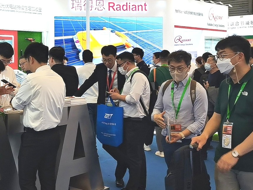
2024 China (Shenzhen) International Semiconductor Exhibition Greater Bay Area Shenzhen Semiconductor Industry Exhibition
Conference theme: Xinlian World Huichuang Future
Time: May 15-17, 2024
Location: Shenzhen International Convention and Exhibition Center (Bao'an New Hall)
Development prospects:
Semiconductors are the core of many industrial equipment and are widely used in core fields such as computers, consumer electronics, network communication, and automotive electronics. Semiconductors are mainly composed of four components: integrated circuits (about 81%), optoelectronic devices (about 10%), discrete devices (about 6%), and sensors (about 3%), so semiconductors and integrated circuits are usually equivalent. Integrated circuits are mainly divided into four categories based on product types: microprocessors (approximately 18%), memory (approximately 23%), logic devices (approximately 27%), and analog devices (approximately 13%).
The semiconductor industry, as the foundation of modern information technology industry, has become a fundamental, strategic, and leading industry for social development and national economy. It is an essential component of modern daily life and future technological progress.
In order to better promote the development of the semiconductor industry, with strong support from national regulatory authorities at all levels, the 2024 China (Shenzhen) International Semiconductor Exhibition will be held grandly from May 15 to 17, 2024 at the Shenzhen International Convention and Exhibition Center (Bao'an New Hall). The exhibition will be held with the aim of "highlighting brand, exploring innovation, and focusing on practical results". With unique creativity, scientific and reasonable integration and excellent services, and a new concept, we will provide exhibitors with a "high-level, high-grade, and high-quality" display and communication stage, creating a top tier event that integrates the scale, value, and authority of the semiconductor industry. We look forward to your participation in this exhibition.
Advantages of the Greater Bay Area:
As China's manufacturing industry has shifted from high-speed growth to high-quality development, since 2013, the Chinese government has successively announced and promoted the "the Belt and Road" initiative and the construction of the "the Belt and Road" Greater Bay Area. The goal is to establish a new economic and trade partnership with countries along the "Belt and Road". At home, through the "Guangdong, Hong Kong and Macao Greater Bay Area", the Chinese government has accelerated the construction of a modern industrial system and multilateral open markets to drive high-quality development through continuous innovation.
The construction of the "Guangdong Hong Kong Macao Greater Bay Area" refers to the development of nine cities in Guangdong Province (including Guangzhou, Shenzhen, Zhuhai, Foshan, Huizhou, Dongguan, Zhongshan, Jiangmen and Zhaoqing) and two special administrative regions of Hong Kong and Macao into world-class city groups and international scientific and technological innovation centers with global influence. By deepening cooperation between Guangdong, Hong Kong and Macao and giving full play to their respective advantages, the Greater Bay Area will promote the coordinated development of regional economy and become the "the Belt and Road" An important support for building a new platform for international economic cooperation. In 2019, the GPD of the Greater Bay Area reached RMB 11.6 trillion, and it is expected to reach RMB 28.9 trillion by 2030, ranking among the top ten economies in the world.
The Guangdong Hong Kong Macao Greater Bay Area gathers high-quality resources from two regions, one province, and nine cities. It will be built into an international science and technology innovation center with global influence, a world-class advanced manufacturing and strategic emerging industry cluster area, and the fourth world-class bay area after New York, San Francisco, and Tokyo, Japan.
Urban clusters with open innovation capabilities and enormous development potential are gathering places for traditional manufacturing industries, including automobile manufacturing, new energy vehicles, semiconductors, household appliances, consumer electronics, electronic information and equipment manufacturing, 5G materials, intelligent manufacturing, high-performance materials, energy conservation and environmental protection, etc.
Exhibition scope:
1. Semiconductor equipment and intelligent equipment: packaging equipment, diffusion equipment, welding equipment, cleaning equipment, testing equipment, refrigeration equipment, oxidation equipment, thinning machine, slicing machine, SMT machine, single crystal furnace, oxidation furnace, grinding machine, heat treatment equipment, lithography machine, etching machine, polishing machine, chamfering machine, ion injection equipment, CVD/PVD equipment, coating/developing machine, front-end testing equipment, wet process equipment, thermal processing, coating equipment Single crystal deposition system, solidification machine, plasma cleaning equipment, cutting machine, loading machine, bonding machine, wire bonding machine, plastic sealing machine, reflow soldering, wave soldering, testing machine, bending equipment, sorting machine, robot automation, machine vision, other materials and electronic special equipment, coupling machine, carrier molding machine, testing equipment, constant temperature and humidity test box, sensor, packaging mold, testing fixture, precision slide table, stepper motor Valves, probe stations, cleanroom equipment, water treatment, etc
2. Wafer manufacturing and packaging: wafer manufacturing, advanced SiP packaging, OSATs, EMS, OEMs, IDMs, silicon wafer and IC packaging carriers, printed circuit boards, packaging substrates and equipment, assembly and testing, packaging design, testing, equipment and application manufacturing and packaging, EDA, MCU, printed circuit boards, etc;
3. Packaging and testing supporting equipment: testing probe table, probe card, testing machine, sorting machine, packaging equipment, packaging substrate, lead frame bonding wire, lead bonding, welding testing, automated testing, laser cutting and other, grinding fluid, scratching fluid, high-temperature sealing film (adhesive) tape, laminated substrate, SMT adhesive, feeding plate, solder wire flow control, quartz graphite, silicon carbide, etc;
4. IC design: IC and related electronic product design, IC product and application technology, IC testing methods and instruments, IC design and design tools, IC manufacturing and packaging, EDA, IP design, embedded software, digital circuit design, analog and mixed signal circuit design, integrated circuit layout design, IDM, Fabless factory, etc;
5. Integrated circuits: wafer manufacturing plants, wafer foundries, analog integrated circuits, digital integrated circuits, mixed digital and analog integrated circuit manufacturing, integrated circuit terminal products, etc;
6. Semiconductor materials: silicon wafers and silicon-based materials, silicon wafers, silicon wafers, monocrystalline silicon, silicon wafers, germanium silicon materials, S01 materials, silicon materials and compound semiconductor materials for solar cells, quartz products, graphite products, anti-static materials, photoresists and their supporting reagents, wafer tapes, photomask plates, electronic gases, special chemical gases, CMP polishing materials, packaging substrates, lead frames, bonding wires, packaging materials Ceramic substrates, chip bonding materials, photoresist materials, wet electronic chemicals, sputtering targets, sealing materials, slicing, grinding, polishing, thin films, etc;
7. Third generation semiconductors: Third generation semiconductors such as silicon carbide SiC, gallium nitride GaN, wafers, substrates, packaging, testing, optoelectronic devices (light-emitting diodes LED, laser LD, detector UV), power electronic devices (diodes, MOSFET, JFET, BJT, IGBT, GTO, ETO, SBD, HEMT, etc.), microwave and radio frequency devices (HEMT, MMIC, etc.);
8. Electronic components: resistors, capacitors, potentiometers, electronic tubes, heat sinks, electromechanical components, connectors, semiconductor discrete devices/IGBT, electroacoustic devices, laser devices, electronic display devices, optoelectronic devices, sensors, power supplies, switches, micro motors, electronic transformers, relays, printed circuit boards, integrated circuits, various circuits, piezoelectric, crystal, quartz, ceramic magnetic materials Printed circuit substrates, electronic functional process specific materials, electronic adhesive (tape) products, electronic chemical materials and components, passive devices, 5G core components, special electronics, components, power management, storage, connectors, cables, plug-in devices, crystal oscillators, resistors, potentiometer magnetic components, filtering components, PCB boards, motor fans, electroacoustic devices, display devices, diodes, transistor filtering components, etc;
Sponsorship Program:
In order to facilitate well-known enterprises to leverage the international influence of this exhibition, showcase their strength, and enhance their brand image, the organizing committee has set up a special exhibition sponsorship plan. An efficient sponsorship program will bring you more business opportunities and enhance your participation before, during, and after the exhibition.
Four levels are specially designated: Diamond, Platinum, Gold, and Silver (detailed plans are available upon request). Sponsors will receive the following benefits:
● Engage more target customers through effective market exposure ● Achieve higher exposure rates than competitors
● Participate in industry events with an industry attitude ● Enhance brand image and awareness
● Establish a sales network through a new platform to increase trade opportunities ● Obtain more information on buyers and professional sellers
Exhibition reminder:
1. Please fill out the "Exhibition Application and Contract" form carefully and stamp it with the official seal before returning it to the organizing committee.
2. After applying for a booth, exhibitors are required to wire transfer the booth fees to the designated account of the conference within 3 working days. After the remittance, the remittance receipt should be returned to the organizing committee for verification; If payment is not made in a timely manner within the specified time, the organizing committee will not retain the original booth.
3. Principle of booth allocation: "Apply first, pay first, and arrange first".
4. In order to ensure the overall image of the conference, the organizing committee reserves the ultimate right to adjust some of the exhibitors' booths.
Contact information of the organizing committee:
Postal code: 201908
Contact person: Mr. Lin
Phone: 15800669522
Scope

Exhibition scope:
1. Semiconductor equipment and intelligent equipment: packaging equipment, diffusion equipment, welding equipment, cleaning equipment, testing equipment, refrigeration equipment, oxidation equipment, thinning machine, slicing machine, SMT machine, single crystal furnace, oxidation furnace, grinding machine, heat treatment equipment, lithography machine, etching machine, polishing machine, chamfering machine, ion injection equipment, CVD/PVD equipment, coating/developing machine, front-end testing equipment, wet process equipment, thermal processing, coating equipment Single crystal deposition system, solidification machine, plasma cleaning equipment, cutting machine, loading machine, bonding machine, wire bonding machine, plastic sealing machine, reflow soldering, wave soldering, testing machine, bending equipment, sorting machine, robot automation, machine vision, other materials and electronic special equipment, coupling machine, carrier molding machine, testing equipment, constant temperature and humidity test box, sensor, packaging mold, testing fixture, precision slide table, stepper motor Valves, probe stations, cleanroom equipment, water treatment, etc
2. Wafer manufacturing and packaging: wafer manufacturing, advanced SiP packaging, OSATs, EMS, OEMs, IDMs, silicon wafer and IC packaging carriers, printed circuit boards, packaging substrates and equipment, assembly and testing, packaging design, testing, equipment and application manufacturing and packaging, EDA, MCU, printed circuit boards, etc;
3. Packaging and testing supporting equipment: testing probe table, probe card, testing machine, sorting machine, packaging equipment, packaging substrate, lead frame bonding wire, lead bonding, welding testing, automated testing, laser cutting and other, grinding fluid, scratching fluid, high-temperature sealing film (adhesive) tape, laminated substrate, SMT adhesive, feeding plate, solder wire flow control, quartz graphite, silicon carbide, etc;
4. IC design: IC and related electronic product design, IC product and application technology, IC testing methods and instruments, IC design and design tools, IC manufacturing and packaging, EDA, IP design, embedded software, digital circuit design, analog and mixed signal circuit design, integrated circuit layout design, IDM, Fabless factory, etc;
5. Integrated circuits: wafer manufacturing plants, wafer foundries, analog integrated circuits, digital integrated circuits, mixed digital and analog integrated circuit manufacturing, integrated circuit terminal products, etc;
6. Semiconductor materials: silicon wafers and silicon-based materials, silicon wafers, silicon wafers, monocrystalline silicon, silicon wafers, germanium silicon materials, S01 materials, silicon materials and compound semiconductor materials for solar cells, quartz products, graphite products, anti-static materials, photoresists and their supporting reagents, wafer tapes, photomask plates, electronic gases, special chemical gases, CMP polishing materials, packaging substrates, lead frames, bonding wires, packaging materials Ceramic substrates, chip bonding materials, photoresist materials, wet electronic chemicals, sputtering targets, sealing materials, slicing, grinding, polishing, thin films, etc;
7. Third generation semiconductors: Third generation semiconductors such as silicon carbide SiC, gallium nitride GaN, wafers, substrates, packaging, testing, optoelectronic devices (light-emitting diodes LED, laser LD, detector UV), power electronic devices (diodes, MOSFET, JFET, BJT, IGBT, GTO, ETO, SBD, HEMT, etc.), microwave and radio frequency devices (HEMT, MMIC, etc.);
8. Electronic components: resistors, capacitors, potentiometers, electronic tubes, heat sinks, electromechanical components, connectors, semiconductor discrete devices/IGBT, electroacoustic devices, laser devices, electronic display devices, optoelectronic devices, sensors, power supplies, switches, micro motors, electronic transformers, relays, printed circuit boards, integrated circuits, various circuits, piezoelectric, crystal, quartz, ceramic magnetic materials Printed circuit substrates, electronic functional process specific materials, electronic adhesive (tape) products, electronic chemical materials and components, passive devices, 5G core components, special electronics, components, power management, storage, connectors, cables, plug-in devices, crystal oscillators, resistors, potentiometer magnetic components, filtering components, PCB boards, motor fans, electroacoustic devices, display devices, diodes, transistor filtering components, etc;
Costs & Precautions
Contact
- Telephone:15800669522
- Contact:Mr. Lin
- Mobile:15800669522
- Address:No.1 Zhancheng Road, Fuhai Street, Bao'an District, Shenzhen
Disclaimer
The information on this site comes from the network and related members, and the website has done its duty to review it. Due to the uncontrollability of the process of organizing the exhibition, some of the exhibition information in the station may change the subject matter, Extending or cancelling the event, please exhibitors and visitors must check with each other again before exhibiting! All the exhibitions in this site are not hosted/co-organized or organized, if there are any disputes during the exhibition, please hold the main responsibility of the exhibition organization! QQ Email: 523138820@qq.com WeChat: 523138820 Mobile: 15313206870

